UPD3739 Ver la hoja de datos (PDF) - NEC => Renesas Technology
Número de pieza
componentes Descripción
Fabricante
UPD3739 Datasheet PDF : 24 Pages
| |||
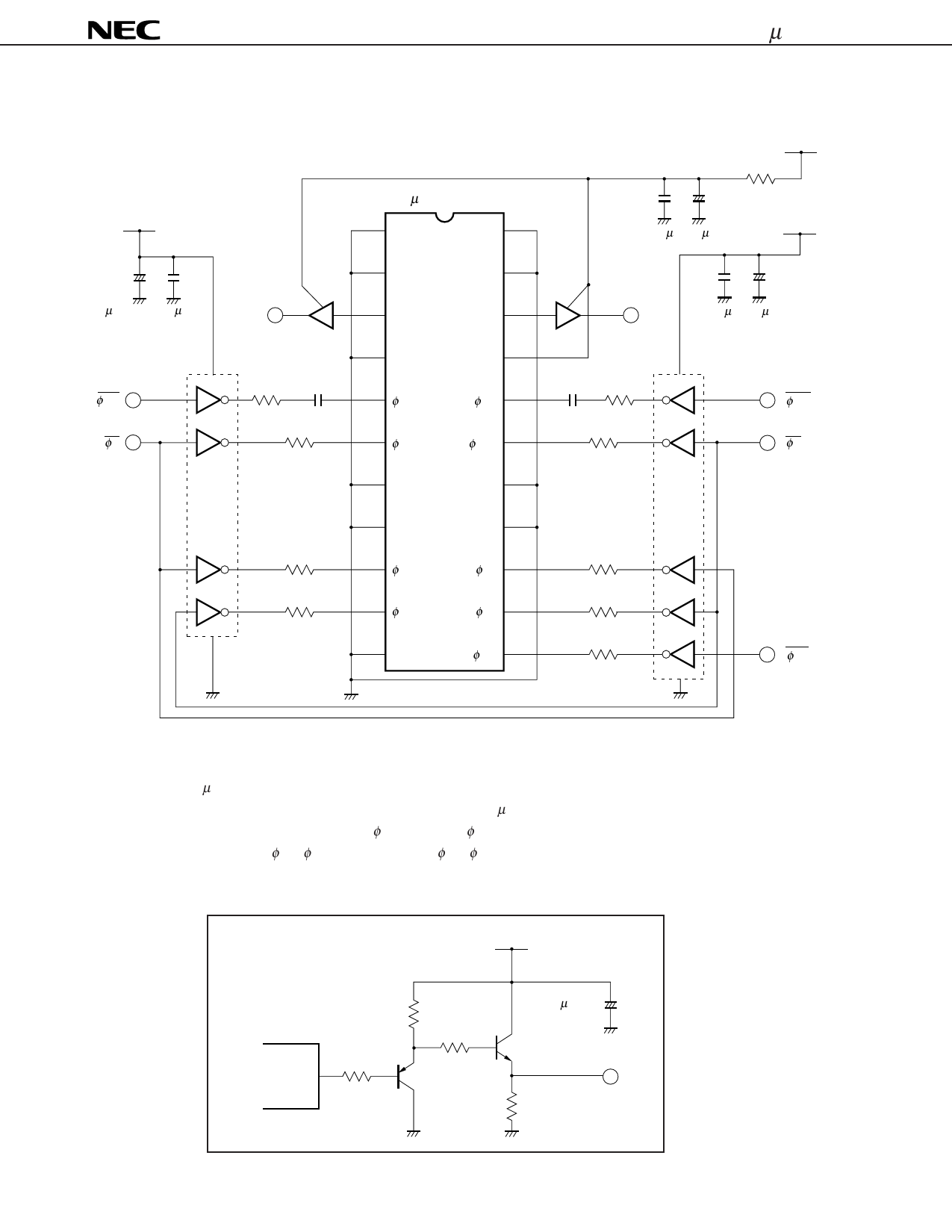
µPD3739
APPLICATION CIRCUIT EXAMPLE (Out of phase operation)
+5 V
+
10 µ F/16 V 0.1 µ F
φ R1
φ2
µ PD3739
1
GND
22
NC
2
NC
21
NC
+12 V
10 Ω
+
0.1 µ F 47µF/25 V
+5 V
+
3
20
B1
VOUT1
VOUT2
B2
0.1 µ F 10 µF/16 V
4
NC
19
VOD
200 Ω 1000 pF
5 φ R1
φR2 18
1000 pF 200 Ω
φR2
47 Ω
6
φ 2L1
17
φ 1L2
47 Ω
φ1
7
NC
16
NC
8
NC
15
NC
2Ω
9
14
2Ω
φ 21
φ 22
2Ω
10
13
2Ω
φ 11
φ 12
11
NC
φTG 12
2Ω
φTG
Remarks 1. The µPD3739 can be operated leaving pin 2 (NC) unconnected, and connecting pin 4 (NC) and pin 11
(NC) to a +12 V power supply (when replaces the µPD35H71A).
2. It is recommended that pins 6 (φ2L1) and 17 (φ1L2) each is separately driven a driver other than that
of pins 10, 13 (φ11, φ12) and pins 9, 14 (φ21, φ22).
3. The inverters shown in the above application circuit example are the 74AC04.
B1, B2 EQUIVALENT CIRCUIT
+12 V
CCD
VOUT
4.7 kΩ
110 Ω
47 Ω
2SA1005
47 µF/25V +
2SC945
1 kΩ
18
Share Link: 