UPD16705N-XXX Ver la hoja de datos (PDF) - NEC => Renesas Technology
Número de pieza
componentes Descripción
Fabricante
UPD16705N-XXX Datasheet PDF : 12 Pages
| |||
µPD16705
3. PIN FUNCTIONS
Pin Symbol
Pin Name
I/O
Description
O1 to O263 Driver output
O These pins output scan signals that drive the vertical direction (gate lines) of a
TFT-LCD. The output signals changes in synchronization with the rising edge of
shift clock CLK. The driver output amplitude is VDD2 to VEE.
R,/L
Shift direction select
I The shift direction control pin of shift resister.
input
R,/L = H (right shift): STVR → O1 → O263 → STVL
R,/L = L or Open (left shift): STVL → O263 → O1 → STVR
STVR,
STVL
Start pulse
input/output
I/O This is the input of the internal shift register. The start pulse is read at the rising
edge of shift clock CLK, and scan signals are output from the driver output pins.
The input level is a VDD1 to VSS (logic level). When in MODE = H, the start pulse is
output at the falling edge of the 263rd clock of shift clock CLK, and is cleared at
the falling edge of the 264th clock. The output level is VDD1 to VSS (logic level).
CLK
Shift clock input
I This pin inputs a shift clock to the internal shift register. The shift operation is
performed in synchronization with the rising edge of this input.
OE1,
OE2,
OE3
Output enable input
I When this pin goes high level, the driver output is fixed to VEE level. The shift
register is not cleared. CLK is asynchronous in the clock. Note that the output
terminal, which can be controlled by the enable signal changes, refers to 4.
RELATIONS OF ENABLE INPUT AND OUTPUT TERMINAL.
/AO
All-on control
I When this pin goes low level, all driver output is fixed to VDD2 level. The shift
register is not cleared. This pin has priority over OE1 to OE3. /AO is pulled up to
VDD1 inside the IC. CLK is asynchronous in the clock.
MODE
Selection of number of I
outputs
MODE = VDD1 or open: 263 outputs
MODE = VSS: 256 outputs (driver output pins O129 to O135 are invalid.)
Input level is VDD1 to VSS (logic level). MODE is pulled up to VDD1 inside the IC.
VDD1
Logic power supply
- 2.3 to 3.6 V
VDD2
Driver positive power
- 15 to 25 V. The driver output: high level
supply
VSS
Logic ground
- Connect this pin to the ground of the system.
VEE
Negative power
- –15 to –5 V. The driver output: low level
supply for internal
operation
Cautions 1. To prevent latch-up, turn on power to VDD1, VEE, VDD2, and logic input in this order. Turn off
power in the reverse order. These power up/down sequence must be observed also during
transition period.
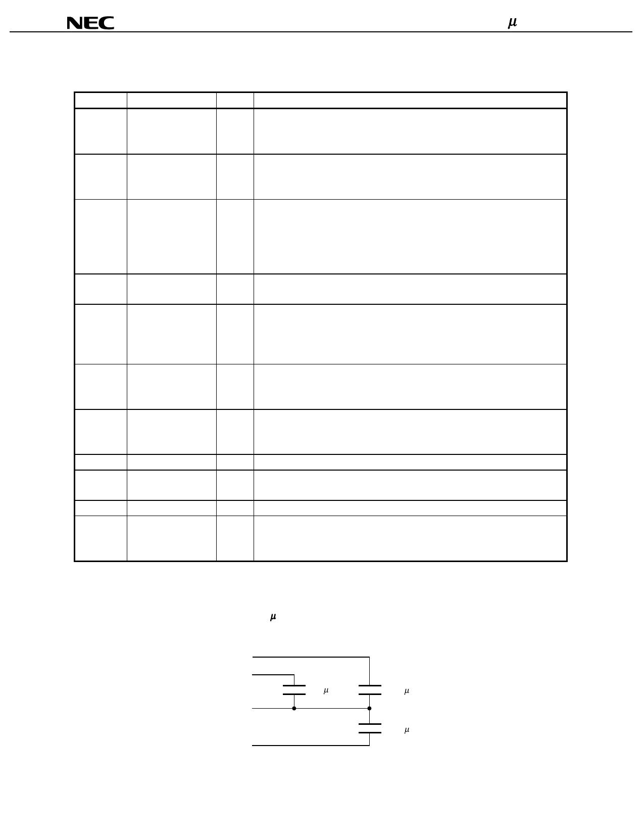
2. Insert a capacitor of about 0.1 µF between each power line, as shown below, to secure noise
margin such as VIH and VIL.
VDD2
VDD1
VSS
VEE
0.1 µ F
0.1 µF
0.1 µF
4
Data Sheet S15818EJ1V0DS
Share Link: 