UPD16704P Ver la hoja de datos (PDF) - NEC => Renesas Technology
Número de pieza
componentes Descripción
Fabricante
UPD16704P Datasheet PDF : 14 Pages
| |||
µ PD16704
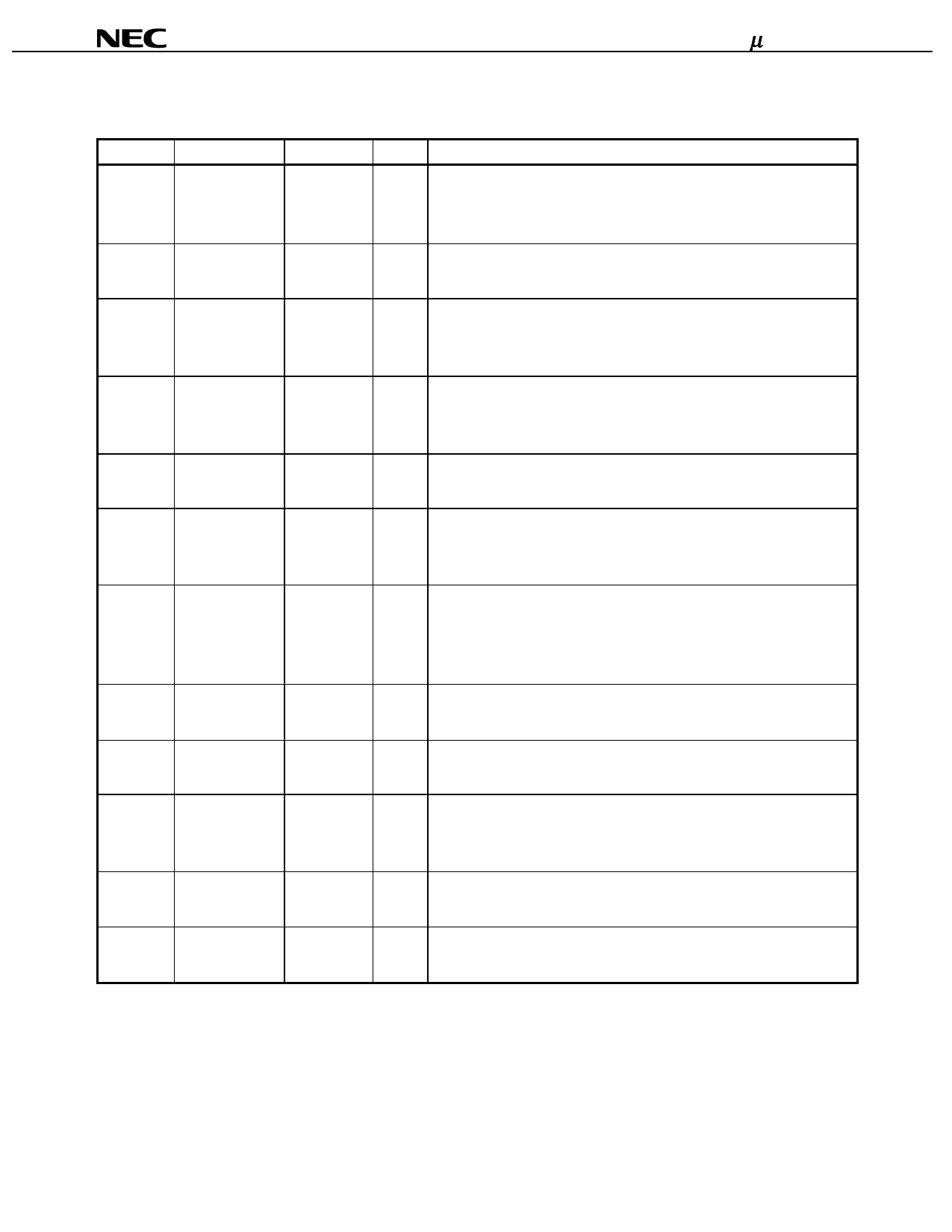
3. PIN FUNCTIONS
Pin Symbol
Pin Name
O1 to O240 Driver output
Pad No
294 - 55
(1/2)
I/O
Description
Output These pins output scan signals that drive the vertical direction (gate lines) of
a TFT-LCD. The output signals change in synchronization with the rising
edge of shift clock CLK. The driver output amplitude is VDD2 to VEE2.
R,/L
Shift direction
select input
18, 19
Input R,/L = H (right shift) : STV → O1 → O240
R,/L = L (left shift) : STV → O240 → O1
STV
Start pulse
input/output
20, 21
I/O This is the input of the internal shift register. The start pulse is written at the
rising edge of shift clock CLK. The pulse range is less than one cycle of
CLK. The input level is a VDD1 to VSS (logic level).
CLK
Shift clock input
22, 23
Input This pin inputs a shift clock to the internal shift register.
The shift operation is performed in synchronization with the rising edge of
this input.
OE
Output enable
26, 27
Input When this pin goes low level, the driver output is fixed to VEE2 level.
input
The shift register is not cleared. Refer to 4. TIMING CHART for details.
DS
Double scan
control input
16, 17
Input
This pin outputs scan signals simultaneously from two outputs in
synchronization with the rise of CLK when DS = H is written. Refer to 4.
TIMING CHART for details.
DSOE
VCC,
VCCC
Double scan pulse
width control input
28, 29
IC internal
reference voltage
34, 35,
36, 37
Input
This pin controls the fall timing of one of the scan signals (the output side in
normal scan mode) when the DS signal is used to output scan signals
simultaneously from two outputs. This signal is input asynchronously to the
clock. Refer to 4. TIMING CHART for details.
– Short the VCC pin to the VCCC pin so that these pins are in a floating state.
TEST1,
TEST2
TEST pins
1, 2,
47, 48
– Short TEST1 and TEST2 separately inside the IC. These pins are not
connected to any other pins inside the IC.
Dummy
Dummy pin
11, 24, 25, 38, – No dummy pins are connected to any other pins inside the IC.
49, 50, 54,
295, 299, 300
VDD1
Logic power
supply
12 - 15
– 3.3 ± 0.3 V
VDD2
Driver positive
51 - 53,
– 15 to 25 V
power supply
296 - 298
The driver output: high level
Data Sheet S15809EJ1V0DS
7
Share Link: 