UPD160062N Ver la hoja de datos (PDF) - NEC => Renesas Technology
Número de pieza
componentes Descripción
Fabricante
UPD160062N Datasheet PDF : 18 Pages
| |||
µ PD160062
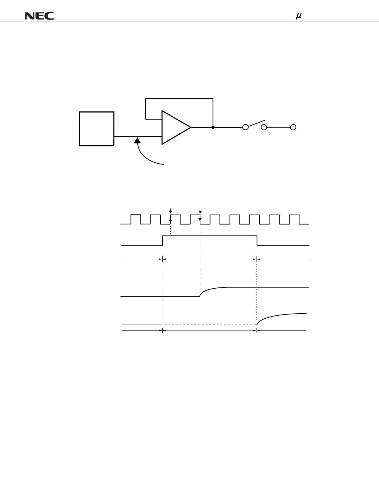
8. RELATIONSHIP BETWEEN STB, CLK AND OUTPUT WAVEFORM
The output voltage is written to the LCD panel synchronized with the STB falling edge.
Figure 8−1. Output Circuit Block Diagram
DAC
Output Amp.
−
+
SW1
Sn
(VX)
VAMP(IN)
Figure 8−2. Output Circuit Timing Waveform
CLK
(External input)
[1]
[2]
STB
(External input)
SW1: ON
SW1: OFF
SW1: ON
VAMP(IN)
Sn
(VOUT: External output)
Output
Hi-Z
Output
Remarks 1. STB = L: SW1 = ON, STB = H: SW1 = OFF
2. STB = H is acknowledged at timing [1] .
3. The display data latch is completed at timing [2] and the input voltage (VAMP(IN): gray-scale level
voltage) of the output amplifier changes.
10
Data Sheet S16449EJ1V0DS
Share Link: 