UMA1005 Ver la hoja de datos (PDF) - Philips Electronics
Número de pieza
componentes Descripción
Fabricante
UMA1005 Datasheet PDF : 24 Pages
| |||
Philips Semiconductors
Dual low-power frequency synthesizer
Preliminary specification
UMA1005T
FUNCTIONAL DESCRIPTION
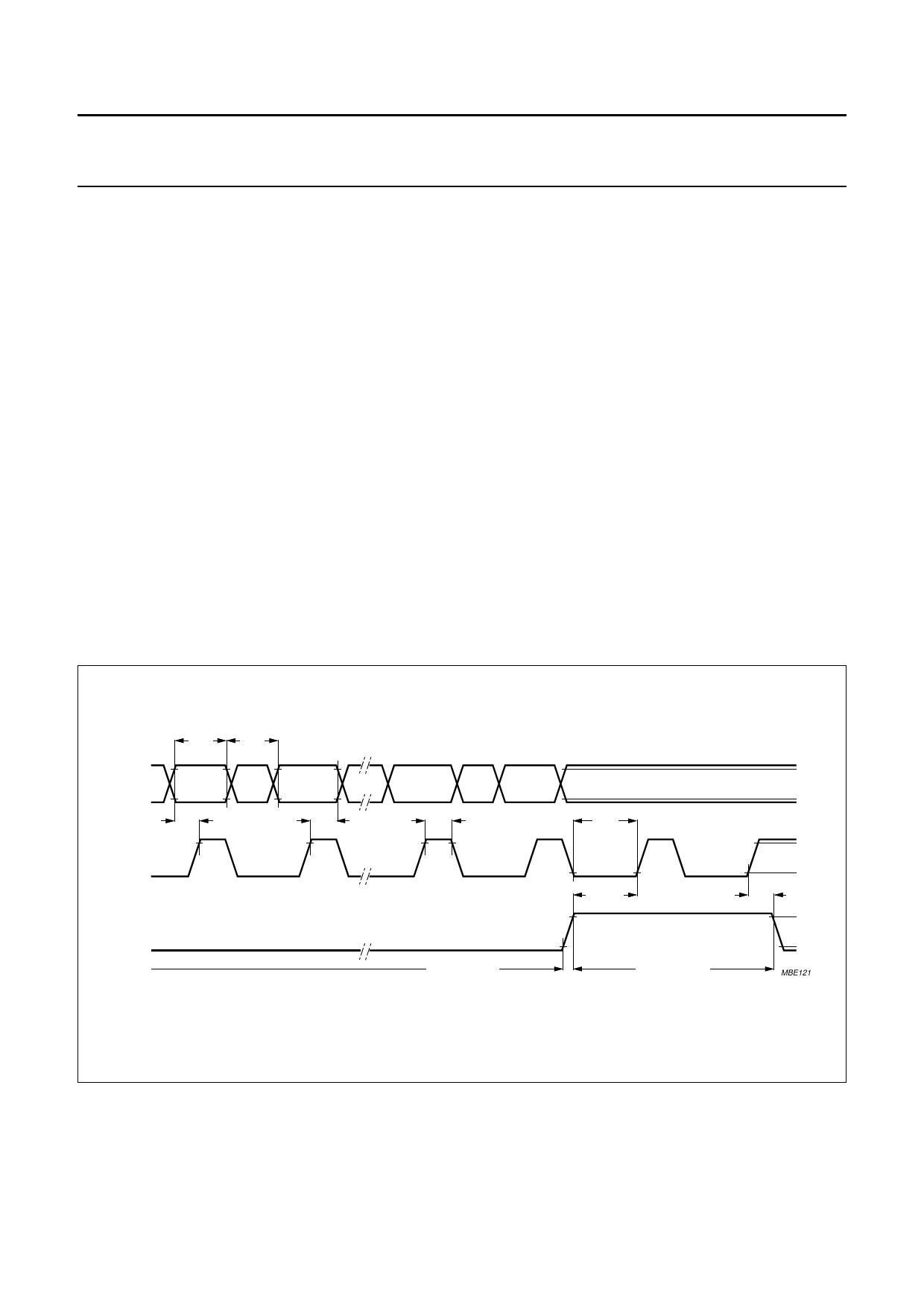
Serial programming input
The serial input is a 3-wire input (CLOCK, STROBE and
DATA) to program all counter ratios, DACs, selection and
enable bits. The programming data is structured into
24 or 32-bit words. Each word includes 1 or 4 address
bits. Figure 3 shows the timing diagram of the serial input.
When the STROBE = LOW, the clock driver is enabled
and on the positive edges of the CLOCK the signal on the
DATA input is clocked into a shift register. When the
STROBE = HIGH, the clock is disabled and the data in the
shift register remains stable. Depending on the
1 or 4 address bits the data is latched into different
working registers or temporary registers. In order to fully
program the synthesizer, 4 words must be sent:
1. D word.
2. C word.
3. B word.
4. A word.
Figure 4 shows the format and the contents of each word.
The E word is for testing purposes only. The E (test) word
is reset when programming the D word. The data for NM4,
CN and PR is stored by the B word temporary registers.
When the A word is loaded, the data of these temporary
registers is loaded together with the A word into the work
registers which avoids false temporary main divider input.
CN is only loaded from the temporary registers when a
short 24-bit A0 word is used. CN will be directly loaded by
programming a long 32-bit A1 word. The flag LONG in the
D word determines whether A0 (LONG = 0) or A1
(LONG = 1) format is applicable.
The A word contains new data for the main divider. The
A word is loaded only when a main divider synchronization
signal is also active, to avoid phase jumps when
reprogramming the main divider. The synchronization
signal is generated by the main divider. It disables the
loading of the A word each main divider cycle during
maximum 300 main divider input cycles. To make sure
that the A word will be correctly loaded the STROBE signal
must be HIGH for at least 300 main divider input cycles.
Programming the A word also means that the main charge
pumps on outputs PHP and PHI are set into the speed-up
mode as long as the STROBE remains HIGH.
handbook, full pagewidth
data
valid
data
change
DATA
D0
D1
t suDA t hDA
CLOCK
STROBE
D30
D31
t HC
clock enabled
shift in data
t LC
t suST
t hST
clock disabled
store data
VH
VL
VH
VL
VH
VL
MBE121
Fig.3 Serial input timing sequence.
November 1994
5
Share Link: 