AT6000 Ver la hoja de datos (PDF) - Atmel Corporation
Número de pieza
componentes Descripción
Fabricante
AT6000 Datasheet PDF : 28 Pages
| |||
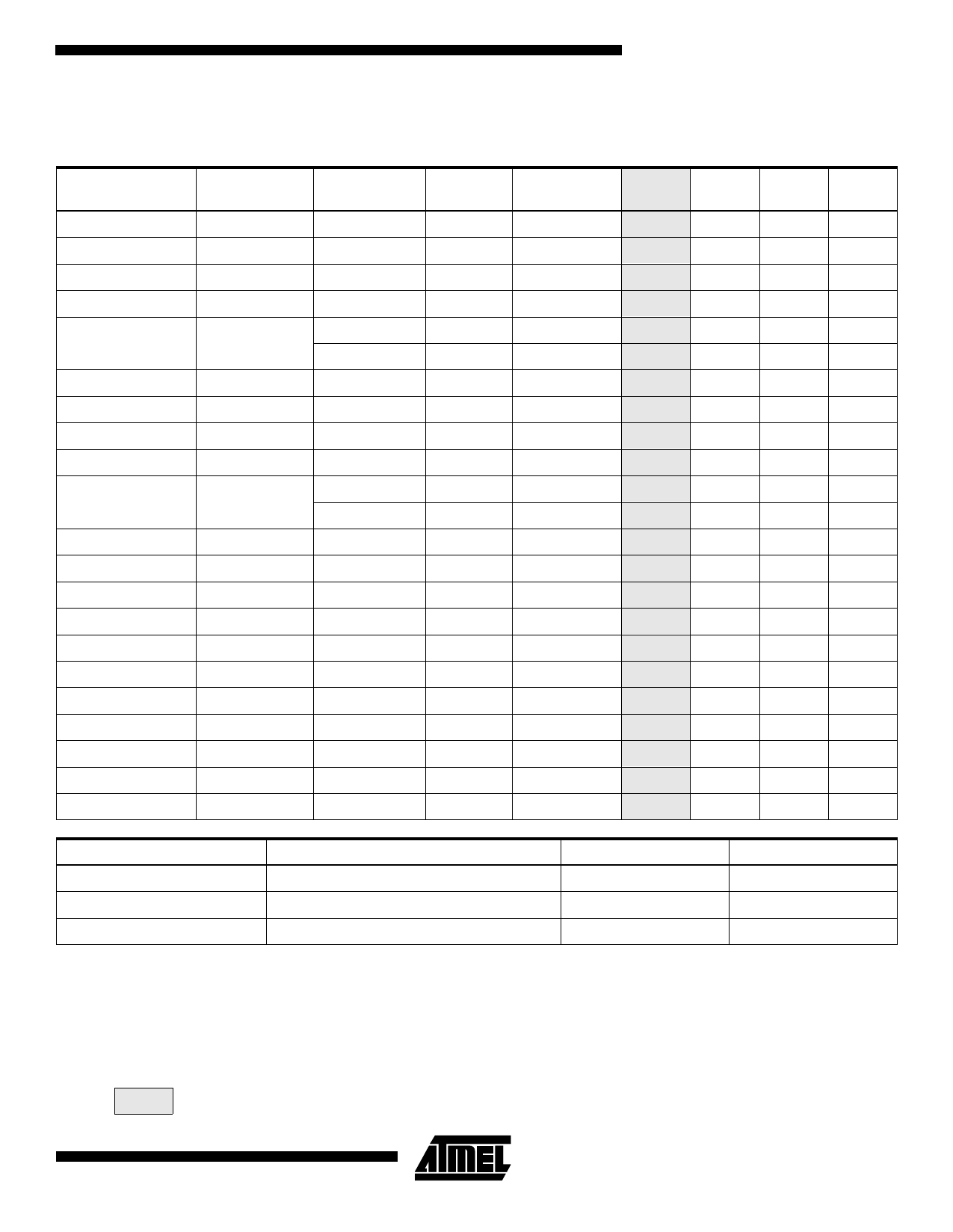
AT6000(LV) Series
AC Timing Characteristics – 5V Operation
Delays are based on fixed load. Loads for each type of device are described in the notes. Delays are in nanoseconds.
Worst case: VCC = 4.75V to 5.25V. Temperature = 0°C to 70°C.
Cell Function
Parameter
From
Load
To
Definition(7)
-1
-2
-4
Units
Wire(4)
tPD (max)(4)
A, B, L
A, B
1
0.8
1.2
1.8
ns
NAND
tPD (max)
A, B, L
B
1
1.6
2.2
3.2
ns
XOR
tPD (max)
A, B, L
A
1
1.8
2.4
4.0
ns
AND
tPD (max)
A, B, L
B
1
1.7
2.2
3.2
ns
MUX
tPD (max)
A, B
A
L
A
1
1.7
2.3
4.0
ns
1
2.1
3.0
4.9
ns
D-Flip-flop(5)
D-Flip-flop(5)
D-Flip-flop
Bus Driver
Repeater
tsetup (min)
thold (min)
tPD (max)
tPD (max)
tPD (max)
A, B, L
CLK
-
CLK
A, B, L
-
CLK
A
1
A
L
2
L, E
E
3
L, E
L
2
1.5
2.0
3.0
ns
0
0
0
ns
1.5
2.0
3.0
ns
2.0
2.6
4.0
ns
1.3
1.6
2.3
ns
1.7
2.1
3.0
ns
Column Clock
tPD (max)
GCLK, A, ES
CLK
3
Column Reset
tPD (max)
GRES, A, EN
RES
3
Clock Buffer(5)
tPD (max)
CLOCK PIN
GCLK
-
Reset Buffer(5)
tPD (max)
RESET PIN
GRES
-
TTL Input(1)
tPD (max)
I/O
A
3
CMOS Input(2)
tPD (max)
I/O
A
3
Fast Output(3)
tPD (max)
A
I/O PIN
4
Slow Output(3)
Output Disable(5)
Fast Enable(3)(5)
tPD (max)
tPXZ (max)
tPXZ (max)
A
I/O PIN
4
L
I/O PIN
4
L
I/O PIN
4
Slow Enable(3)(5)
tPXZ (max)
L
I/O PIN
4
1.8
2.4
3.0
ns
1.8
2.4
3.0
ns
1.6
2.0
2.9
ns
1.5
1.9
2.8
ns
1.0
1.2
1.5
ns
1.3
1.4
2.3
ns
3.3
3.5
6.0
ns
7.5
8.0
12.0
ns
3.1
3.3
5.5
ns
3.8
4.0
6.5
ns
8.2
8.5
12.5
ns
Device
Cell(6)
Cell Types
Wire, XWire, Half-adder, Flip-flop
Outputs
A, B
ICC (max)
4.5 µA/MHz
Bus(6)
Wire, XWire, Half-adder, Flip-flop, Repeater
L
2.5 µA/MHz
Column Clock(6)
Column Clock Driver
CLK
40 µA/MHz
Notes:
1. TTL buffer delays are measured from a VIH of 1.5V at the pad to the internal VIH at A. The input buffer load is constant.
2. CMOS buffer delays are measured from a VIH of 1/2 VCC at the apd to the internal VIH at A. The input buffer load is constant.
3. Buffer delay is to a pad voltage of 1.5V with one output switching.
4. Max specifications are the average of mas tPDLH and tPDHL.
5. Parameter based on characterization and simulation; not tested in production
6. Exact power calculation is available in an Atmel application note.
7. Load Definition: 1 = Load of one A or B input; 2 = Load of one L input; 3 = Constant Load; 4 = Tester Load of 50 pF.
= Preliminary Information
19
Share Link: 