TDA3605Q/N1/S420 Ver la hoja de datos (PDF) - Philips Electronics
Número de pieza
componentes Descripción
Fabricante
TDA3605Q/N1/S420 Datasheet PDF : 16 Pages
| |||
Philips Semiconductors
Multiple voltage regulator with switch
Preliminary specification
TDA3605Q
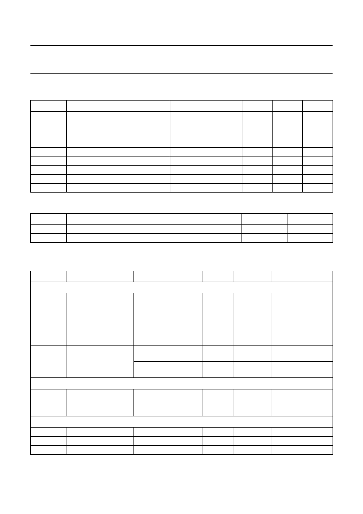
LIMITING VALUES
In accordance with the Absolute Maximum Rating System (IEC 134).
SYMBOL
PARAMETER
CONDITIONS
MIN.
VP
VP
Ptot
Tstg
Tamb
Tj
supply voltage
operating
jump start
load dump protection
reverse battery voltage
total power dissipation
storage temperature
ambient temperature
junction temperature
−
t ≤ 10 minutes
−
during ≤50 ms; tr ≥ 2.5 ms −
non-operating
−
−
non-operating
−55
operating
−40
operating
−40
MAX.
UNIT
18
V
30
V
50
V
−18
V
62
W
+150
°C
+85
°C
+150
°C
THERMAL CHARACTERISTICS
SYMBOL
Rth j-c
Rth j-a
PARAMETER
thermal resistance from junction to case
thermal resistance from junction to ambient in free air
VALUE
2
50
UNIT
K/W
K/W
CHARACTERISTICS
VP = 14.4 V; Tamb = 25 °C; see Fig.6; unless otherwise specified.
SYMBOL
PARAMETER
CONDITIONS
MIN.
Supply
VP
supply voltage
operating
11
regulator 2 on
note 1
2.4
jump start
t ≤ 10 minutes
−
load dump protection during ≤50 ms;
−
tr ≥ 2.5 ms
Iq
quiescent current
VP = 12.4 V; note 2;
−
IR2 = 0.1 mA
VP = 14.4 V; note 2;
−
IR2 = 0.1 mA
Schmitt-trigger power supply for switch, regulator 1 and regulator 3
Vthr
rising voltage threshold
4.0
Vthf
falling voltage threshold
3.5
Vhys
hysteresis
−
Schmitt-trigger power supply for regulator 2
Vthr
rising voltage threshold
6.0
Vthf
falling voltage threshold
1.7
Vhys
hysteresis
−
TYP.
14.4
14.4
−
−
500
520
4.5
4.0
0.5
6.5
1.9
4.6
MAX.
18
18
30
50
600
−
5.0
4.5
−
7.1
2.2
−
UNIT
V
V
V
V
µA
µA
V
V
V
V
V
V
1997 Jul 09
7
Share Link: 