80C196EA Ver la hoja de datos (PDF) - Intel
Número de pieza
componentes Descripción
Fabricante
80C196EA Datasheet PDF : 46 Pages
| |||
8xC196EA — AUTOMOTIVE
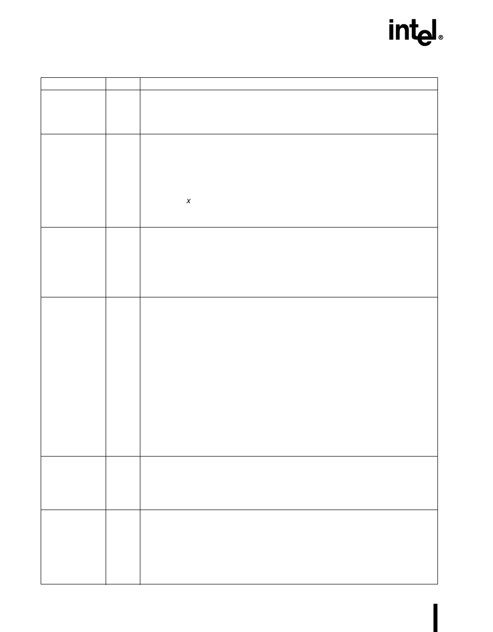
Name
RD#
READY
RESET#
RPD
RXD1:0
SC1:0
12
Type
O
I
I/O
I
I/O
I/O
Table 4. Signal Descriptions (Sheet 6 of 8)
Description
Read
Read-signal output to external memory. RD# is asserted only during external
memory reads.
RD# shares a package pin with P5.3.
Ready Input
This active-high input signal is used to lengthen external memory cycles for
slow memory by generating wait states in addition to the wait states that are
generated internally.
When READY is high, CPU operation continues in a normal manner with wait
states inserted as programmed in the chip configuration registers or the
chip-select x bus control register. READY is ignored for all internal memory
accesses.
READY shares a package pin with P5.6.
Reset
A level-sensitive reset input to and open-drain system reset output from the
microcontroller. Either a falling edge on RESET# or an internal reset turns on a
pull-down transistor connected to the RESET# pin for 16 state times. In the
powerdown and idle modes, asserting RESET# causes the chip to reset and
return to normal operating mode. After a device reset, the first instruction fetch
is from FF2080H (or 1F2080H in external memory).
Return from Powerdown
Timing pin for the return-from-powerdown circuit.
If your application uses powerdown mode, connect a capacitor between RPD
and VSS if either of the following conditions are true.
• the internal oscillator is the clock source
• the phase-locked loop (PLL) circuitry is enabled (see PLLEN signal
description)
The capacitor causes a delay that enables the oscillator and PLL circuitry to
stabilize before the internal CPU and peripheral clocks are enabled.
The capacitor is not required if your application uses powerdown mode and if
both of the following conditions are true.
• an external clock input is the clock source
• the phase-locked loop circuitry is disabled
If your application does not use powerdown mode, leave this pin unconnected.
RPD shares a package pin with P5.7.
Receive Serial Data 0 and 1
In modes 1, 2, and 3, RXD0 and 1 receive serial port input data. In mode 0, they
functions as either inputs or open-drain outputs for data.
RXD0 shares a package pin with P2.1 and RXD1 shares a package pin with
P2.4.
Clock Pins for SSIO0 and 1
For handshaking mode, configure SC1:0 as open-drain outputs.
This pin carries a signal only during receptions and transmissions. When the
SSIO port is idle, the pin remains either high (with handshaking) or low (without
handshaking).
SC0 shares a package pin with P10.0, and SC1 shares a package pin with
P10.2.
ADVANCE INFORMATION
Share Link: 