CGY2010G Ver la hoja de datos (PDF) - Philips Electronics
Número de pieza
componentes Descripción
Fabricante
CGY2010G Datasheet PDF : 12 Pages
| |||
Philips Semiconductors
GSM 4 W power amplifiers
Objective specification
CGY2010G; CGY2011G
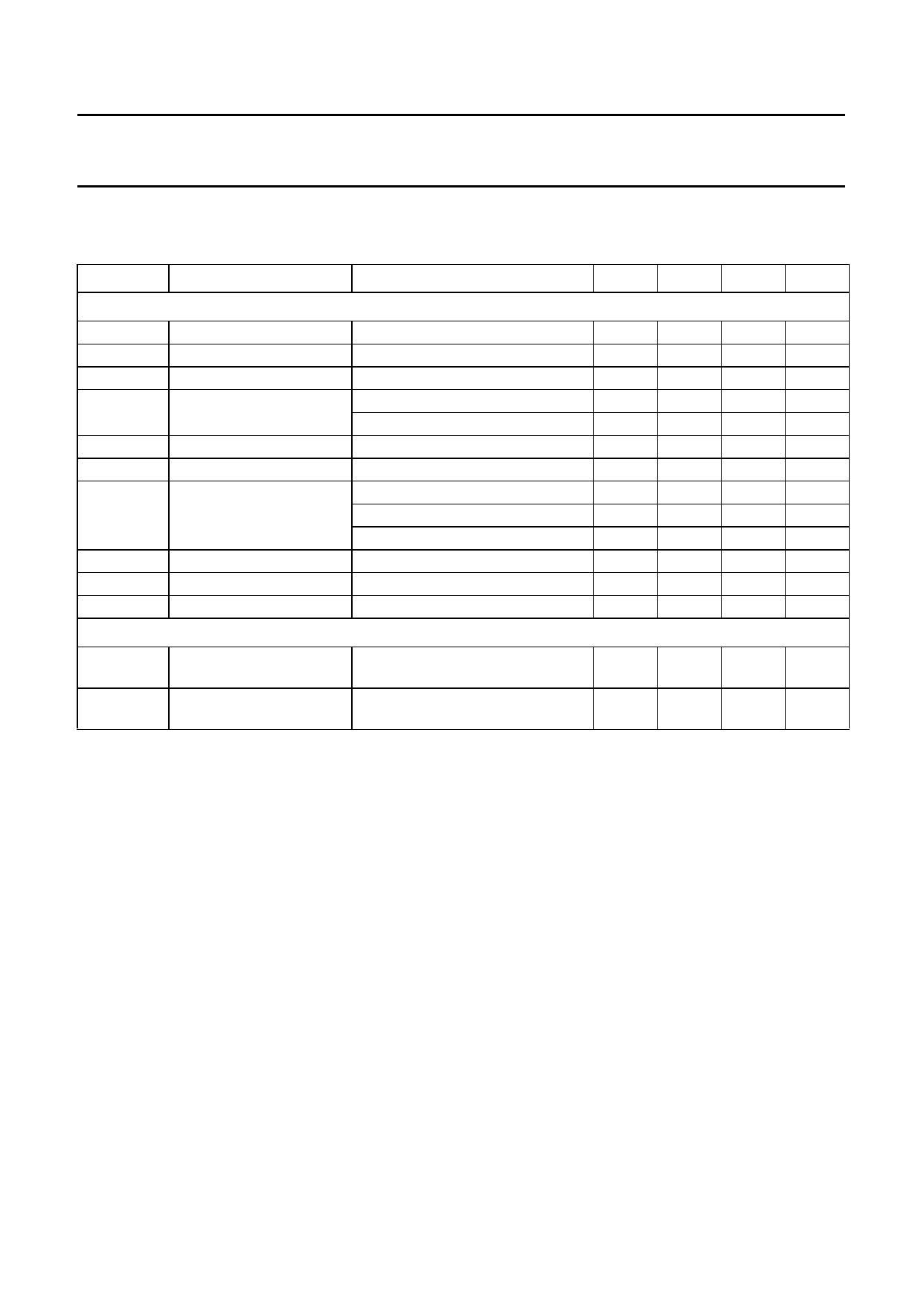
AC CHARACTERISTICS
VDD = 4.5 V; Tamb = 25 °C; general operating conditions applied; unless otherwise specified.
SYMBOL
PARAMETER
CONDITIONS
MIN. TYP.
MAX.
UNIT
Power amplifier
Pin
S11
fRF
Pout(max)
input power
input return loss
RF frequency range
maximum output power
η
Pout(min)
NRX
efficiency
minimum output power
output noise in RX band
H2
H3
Stab
2nd harmonic level
3rd harmonic level
stability
Power sensor driver
Pout(DET)
∆Pout(DET)
sensor driver output
power
driver output power
variation
note 1; 50 Ω source
Tamb = 25 °C; VDD = 4.5 V
Tamb = −20 to +85 °C; VDD = 4.2 V
VDD = 4.2 V
VDD < 0.1 V
fRF = 925 MHz at Pout(max)
fRF = 935 MHz at Pout(max)
fRF = 960 MHz at Pout(max)
note 2
−1.5
−
880
34.5
32.5
−
−
−
−
−
−
−
−
RL = 100 Ω; relative to PA output −
power into 50 Ω load
load VSWR < 6 : 1 at PA output
−
−
−
−
35.5
−
45
−
−
−
−
−33
−40
−
−23
−
+1.5
−6
915
−
−
−
−20
−117
−129
−129
−30
−37
−70
dBm
dB
MHz
dBm
dBm
%
dBm
dBm/Hz
dBm/Hz
dBm/Hz
dBc
dBc
dBc
−
dBc
2
dB
Notes
1. Including the 100 Ω resistor connected in parallel at the power amplifier input on the evaluation board.
2. The device is adjusted to provide nominal value of load power into a 50 Ω load. The device is switched off and a 6 : 1
load replaces the 50 Ω load. The device is switched on and the phase of the 6 : 1 load is varied
360 electrical degrees during a 60 second period.
1996 Jul 08
7
Share Link: 