TA2022 Ver la hoja de datos (PDF) - Unspecified
Número de pieza
componentes Descripción
Fabricante
TA2022 Datasheet PDF : 31 Pages
| |||
Tripath Technology, Inc. - Technical Information
generator is not used, Tripath recommends shorting VN10SW(pin 5) to VN10GND(pin 3) and
VN10FDBK(pin 14) to VN10GND(pin 3). VN10GND should still be connected to the system power
(high current) ground star for noise reasons.
The external VN10 supply must be able to source a maximum of 80mA into the VN10 pin. Thus, a
positive supply must be used. In addition, this supply must be referenced to the VNN rail. If the
external VN10 supply does not track fluctuations in the VNN supply or is not able to source current
into the VN10 pin, the TA2022 will, at the very least, not work, but more likely, be permanently
damaged.
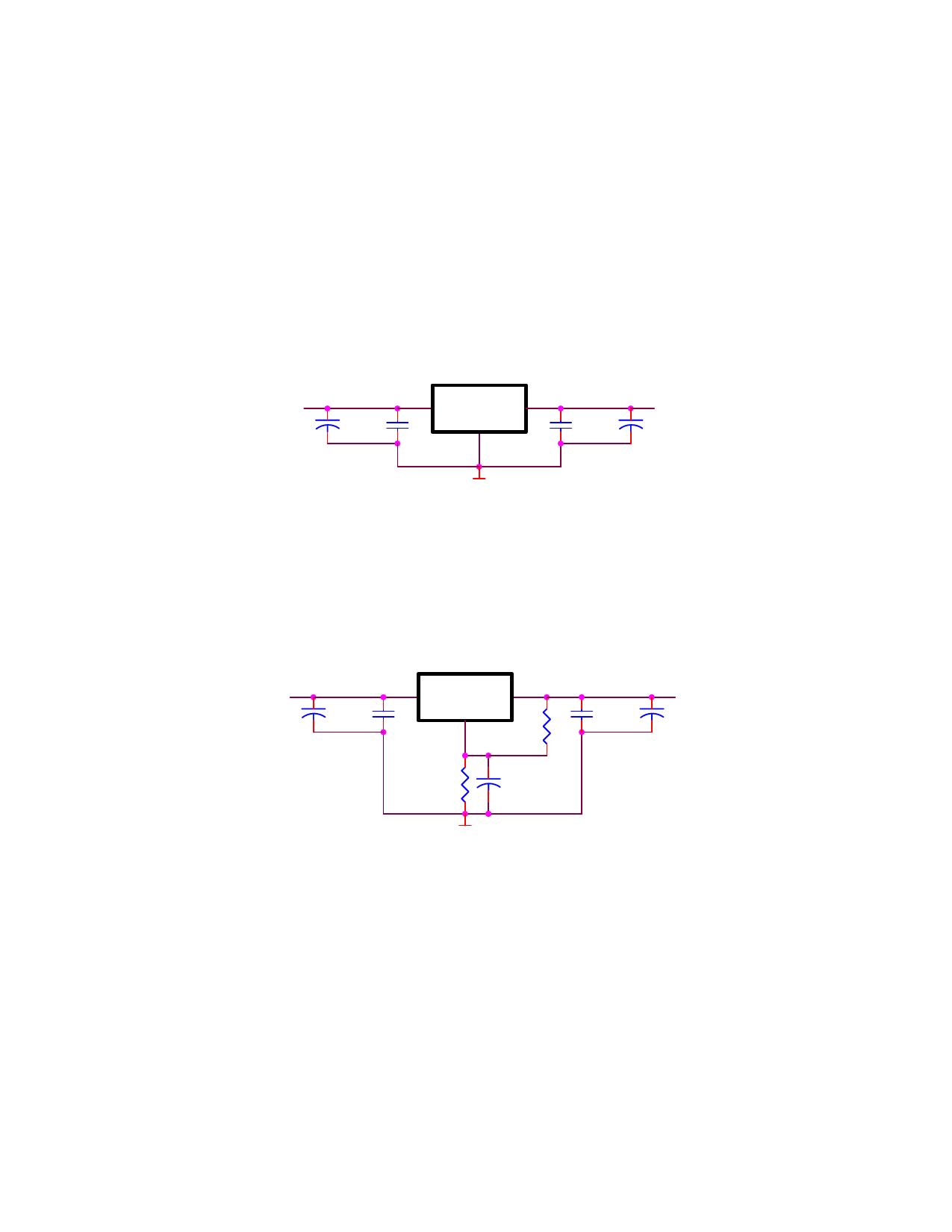
Figure 7 shows a simple circuit for an external VN10 supply. Though simple, there is one problem
with this circuit; the maximum input voltage of the 7810. If the maximum input voltage of the 7810 is
exceeded (typically this voltage is 35V), then the 7810 will be damaged which will likely
cause damage to the TA2022. Thus, this circuit should only be used where the VNN power supply is
well regulated even under heavy load conditions (including the effects of power supply pumping).
TO POWER SUPPLY
"STAR" GND
10uF
0.1uF
VIN
7810
"GND"
VOUT
0.1uF
TO VN10 (PIN 2)
10uF
TO VNN (PIN 8,9)
Figure 7: Simple External VN10 Supply
Figure 8 shows a much more robust VN10 supply. In this case, the maximum supply differential the
LM317 experiences is the input voltage minus the output voltage. The maximum differential
specification is 40V for the LM317. When used as the VN10 supply for the TA2022, the maximum
differential the LM317 will experience is 25V, even at maximum operating voltage of 36V for the
TA2022. As configured, VOUT will be about 10.63V above VNN.
TO POWER SUPPLY
"STAR" GND
10uF
0.1uF
VIN
LM317
VOUT
ADJ
240
0.1uF
TO VN10 (PIN 2)
10uF
1.8k
10uF
TO VNN (PIN 8,9)
Figure 8: Robust External VN10 Supply
It should be noted that the maximum power dissipation for either Figure 6 or Figure 7 is:
PDMAX = (VIN − VOUT) × IOUT ≈ (31V − 11V) × 80mA(max.) = 1.6W
Thus, the LM7810 or LM317 must be sufficiently heat sinked to sustain 80mA in the system ambient
temperature. In the case where multiple TA2022’s are run off the same VN10 generator, the power
dissipation may be prohibitively large for the linear regulator in conjunction with allowable heat sink.
In these cases, a more sophisticated scheme using an additional transformer secondary winding
referenced to VNN may be necessary to minimize the linear regulator power dissipation.
23
TA2022 – KLI/1.2/07-04
Share Link: 