W91030BS Ver la hoja de datos (PDF) - Winbond
Número de pieza
componentes Descripción
Fabricante
W91030BS Datasheet PDF : 31 Pages
| |||
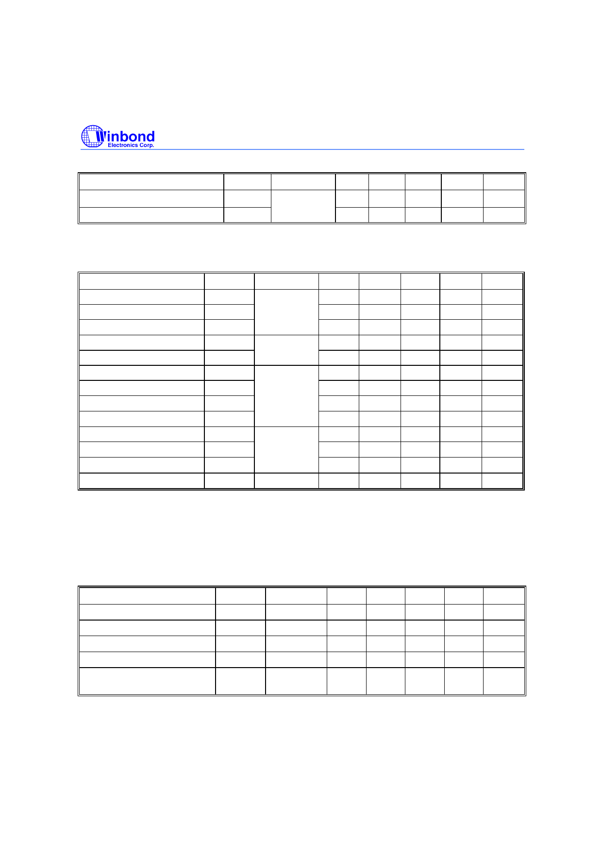
Preliminary W91030B
FSK Detection, continued
PARAMETER
SYMBOL CONDITION MIN. TYP.♣ MAX. UNITS NOTES
Input FSK to FCDN High Delay tCA
FCDN
8
mS
Hysteresis
8
mS
Note: "♣" typical figure are at VDD = 5V and temperature = 25° C are design aids only, not guaranteed and not subject to
production testing.
3-Wire Interface (Mode 0)
PARAMETER
Rise Time
Fall Time
Low Time
Rate
Input FSK to DATA Delay
Rise Time
Fall Time
DATA to DCLK Delay
DCLK to DATA Delay
Frequency
High Time
Low Time
DCLK to FDRN Delay
SYMBOL CONDITION MIN.
tRR
tRF
FDRN
tRL
415
DATA
1188
tIDD
tR
tF
DCLK
tDCD
DATA
6
tCDD
6
fDCLK0
1201.6
tCH
DCLK
415
tCL
415
tCRD DCLK, FDRN 415
TYP.♣
416
1200
1
416
416
1202.8
416
416
416
MAX.
200
200
417
1212
5
200
200
1204
417
417
417
UNITS NOTES
nS
4
nS
4
µS
2
bpS
1
mS
nS
4
nS
4
µS 1, 2, 3
µS 1, 2, 3
Hz
2
µS
2
µS
2
µS
2
Notes:
"♣" Ttypical figure are for VDD = 5V and temperature = 25° C, are design aids only, not guaranteed and not subject to
production testing.
1. FSK input data rate at 1200 +/-12 baud.
2. OSCI frequency at 3.579545 MHz +/-0.1%.
3. Function of signal condition.
4. 50 pF loading.
3-Wire Interface (Mode 1)
PARAMETER
Frequency
Duty Cycle
Rise Time
DCLK Low Set-up to FDRN
DCLK Low Hold Time After
FDRN
SYMBOL CONDITION
fDCLK1
DCLK
tR1
tDDS
DCLK,
tDDH
FDRN
MIN.
30
500
500
TYP.♣
MAX.
1
70
20
UNITS NOTES
MHz
%
nS
nS
nS
Note: "♣" typical figure are at VDD = 5V and temperature = 25° C are design aids only, not guaranteed and not subject to
production testing.
- 17 -
Publication Release Date: March 2000
Revision A1
Share Link: 