S-1167B49-I6T2G Ver la hoja de datos (PDF) - Seiko Instruments Inc
Número de pieza
componentes Descripción
Fabricante
S-1167B49-I6T2G
Seiko Instruments Inc

S-1167B49-I6T2G Datasheet PDF : 31 Pages
| |||
ULTRA LOW CURRENT CONSUMPTION, HIGH RIPPLE REJECTION AND LOW DROPOUT CMOS VOLTAGE REGULATOR
Rev.2.3_00
S-1167 Series
Operation
1. Basic Operation
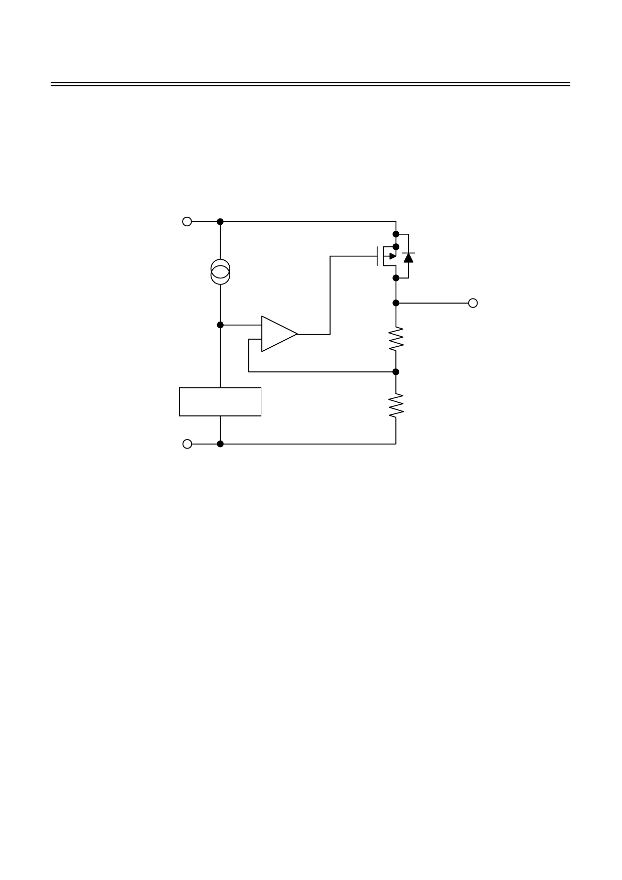
Figure 12 shows the block diagram of the S-1167 Series.
The error amplifier compares the reference voltage (Vref) with Vfb, which is the output voltage resistance-divided by
feedback resistors Rs and Rf. It supplies the output transistor with the gate voltage necessary to ensure a certain
output voltage free of any fluctuations of input voltage and temperature.
VIN
*1
Current supply
Error amplifier
Vref
−
+
VOUT
Rf
Vfb
Reference voltage
circuit
Rs
VSS
*1. Parasitic diode
Figure 12
2. Output Transistor
The S-1167 Series uses a low on-resistance P-channel MOS FET as the output transistor.
Be sure that VOUT does not exceed VIN + 0.3 V to prevent the voltage regulator from being damaged due to inverse
current flowing from the VOUT pin through a parasitic diode to the VIN pin.
Seiko Instruments Inc.
13
Share Link: