PCF2119VU-2 Ver la hoja de datos (PDF) - NXP Semiconductors.
Número de pieza
componentes Descripción
Fabricante
PCF2119VU-2 Datasheet PDF : 79 Pages
| |||
NXP Semiconductors
PCF2119x
LCD controllers/drivers
9.3 CGRAM
Up to 16 user defined characters may be stored in the Character Generator RAM
(CGRAM). Some CGRAM characters (see Figure 21) are also used to drive icons:
• 6 CGRAM characters if icons blink and both icon rows are used in the application
• 3 CGRAM characters if no icons blink but both icon rows are used in the application
• 0 CGRAM characters if no icons are driven by the icon rows
When the icons blink option is enabled, double the number of CGRAM characters are
used since both the on and off state of an icon is defined.
The CGROM and CGRAM use a common address space, of which the first column is
reserved for the CGRAM (see Figure 9 to Figure 14).
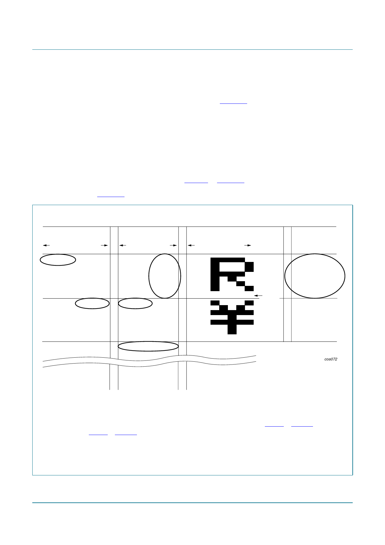
Figure 15 shows the addressing principle for the CGRAM.
character codes
(DDRAM data)
76 5 43 2 10
higher
order
bits
lower
order
bits
00 0 00 0 00
(4)
00 0 00 0 01
(1)
00 0 00 0 10
CGRAM
address
6 5 43 2 10
higher
order
bits
lower
order
bits
00 0 00 0 0
001
010
011
(2)
100
101
110
111
00 0 10 0 0
001
(1)
010
011
100
101
110
(5)
111
0 0 1 00 0 0
001
00 0 01 1 11
00 0 01 1 11
00 0 01 1 11
00 0 01 1 11
1111100
1111101
1111110
1111111
character patterns
(CGRAM data)
4 3 21 0
higher
order
bits
lower
order
bits
0
0 00
0 00
0
0
00
00
0
0 00
0 0 00 0
0 00
0
0
0
00
00
00
00
00
00
0 0 00 0
character
pattern
example 1
cursor
position
character
pattern
example 2
character code
(CGRAM data)
4 3 21 0
1 1 11 0
1 0 00 1
1 0 00 1
1 1 11 0
1 0 10 0
1 0 01 0
1 0 00 1
0 0 0 0 0 (3)
1 0 00 1
0 1 01 0
1 1 11 1
0 0 10 0
1 1 11 1
0 0 10 0
0 0 10 0
0 0 00 0
coa072
(1) Character code bit 0 to bit 3 correspond to CGRAM address bit 3 to bit 6.
(2) CGRAM address bit 0 to bit 2 designate the character pattern line position. The 8th line is the cursor position and display is
performed by logical OR with the cursor. Data in the 8th line will appear in the cursor position. Lines are numbered from 0 to 7.
(3) Character pattern column positions correspond to CGRAM data bit 0 to bit 4, as shown in Figure 9 to Figure 14.
(4) As shown in Figure 9 to Figure 14, CGRAM character patterns are selected when character code bit 4 to bit 7 are all logic 0.
CGRAM data = logic 1 corresponds to selection for display.
(5) Only bit 0 to bit 5 of the CGRAM address are set by the Set_CGRAM command. Bit 6 can be set using the Set_DDRAM
command in the valid address range or by using the auto-increment feature during CGRAM write. All bits from bit 0 to bit 6 can
be read using the BF_AC instruction.
Fig 15. Relationship between CGRAM addresses, data and display patterns
PCF2119X_5
Product data sheet
Rev. 05 — 13 August 2009
© NXP B.V. 2009. All rights reserved.
22 of 79
Share Link: 