NT7502H-BDT Ver la hoja de datos (PDF) - Novatek Microelectronics
Número de pieza
componentes Descripción
Fabricante
NT7502H-BDT Datasheet PDF : 54 Pages
| |||
NT7502
The Display Data Latch Circuit
The display data latch circuit is a latch that temporarily stores the display data output to the liquid crystal driver circuit from the
display data RAM.
Because the display normal/reverse status, display ON/OFF status, and display all points ON/OFF commands control only the
data within the latch, they do not change the data within the display data RAM itself.
The Oscillator Circuit
This is a CR-type oscillator that produces the display clock. The oscillator circuit is only enabled when M/S = “H” and CLS = “H”.
When CLS = “L” the oscillation stops, and the display clock is input through the CL terminal.
Display Timing Generator Circuit
The display timing generator circuit generates the timing signal to the line address circuit and the display data latch circuit using
the display clock. The display data is latched into the display data latch circuit synchronized with the display clock, and is output
to the data driver output terminal. Reading to the display data liquid crystal driver circuits is completely independent of access to
the display data RAM by the MPU. Consequently, even if the display data RAM is accessed asynchronously during liquid
crystal display, there is absolutely no adverse effect (such as flickering) on the display.
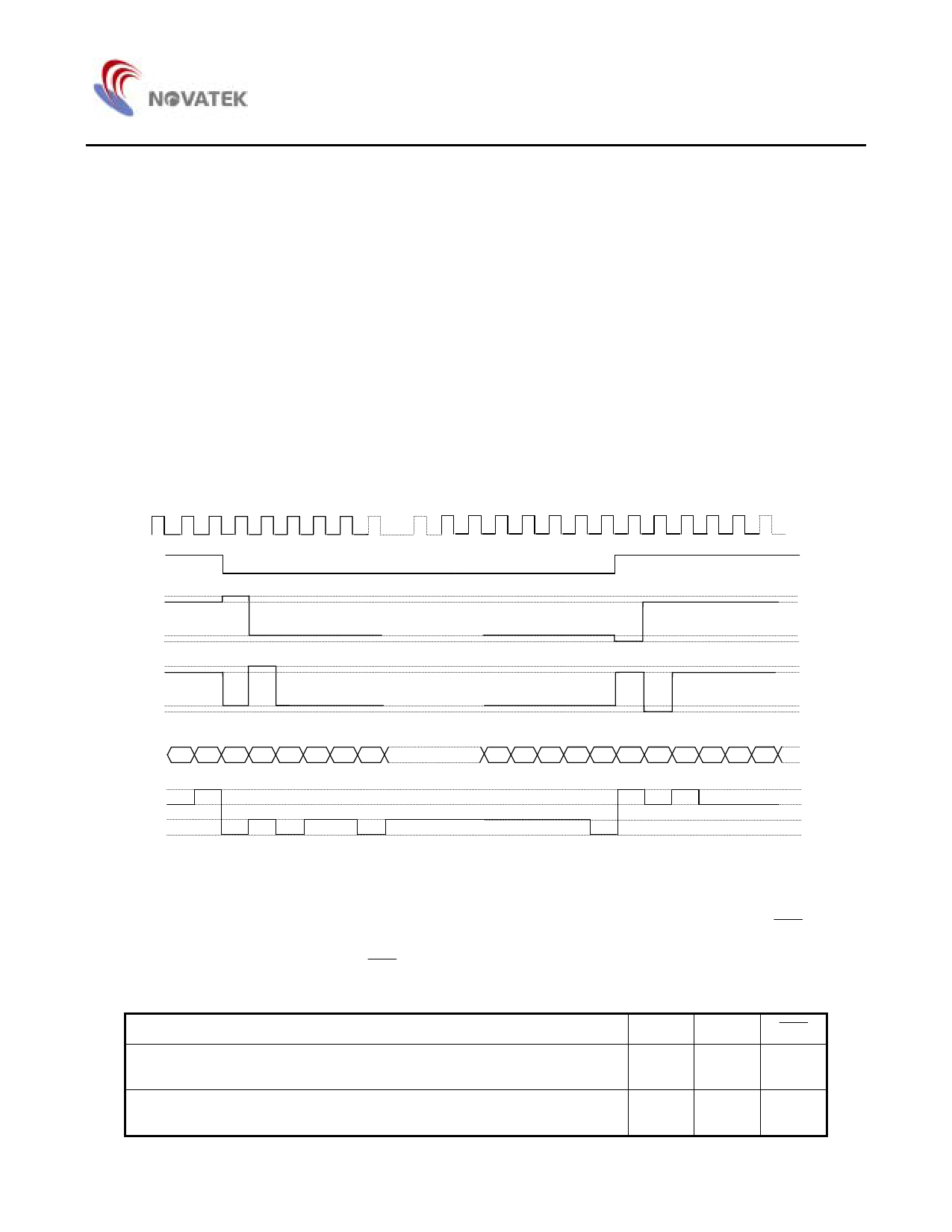
Moreover, the display timing generator circuit generates the common timing and the liquid crystal alternating current signal (FR)
from the display clock. It generates a drive waveform using a 2 frame alternating current drive method, as is shown in Figure 5,
for the liquid crystal drive circuit.
64 65 1
2
3
4
5
6
CL
FR
60 61 62 63 64 65 1
2
3
4
5
6
COM0
COM1
RAM
data
SEGn
V0
V1
V4
VSS
V0
V1
V4
VSS
V0
V2
V3
VSS
Figure. 5
When multiple NT7502 chips are used, the slave chips must be supplied with the display timing signals (FR, CL, DOF ) from the
master chip[s].
Table 5 shows the status of the FR, CL, and DOF signals.
Table. 5
Master (M/S = “H”)
Slave (M/S = “L”)
Operating Mode
The internal oscillator circuit is enabled (CLS = “H”)
The internal oscillator circuit is disabled (CLS = “L”)
The internal oscillator circuit is disabled (CLS = “H”)
The internal oscillator circuit is disabled (CLS = “L”)
FR
Output
Output
Input
Input
CL
Output
Input
Input
Input
DOF
Output
Output
Input
Input
14
Share Link: 