HA-5340 Ver la hoja de datos (PDF) - Intersil
Número de pieza
componentes Descripción
Fabricante
HA-5340 Datasheet PDF : 8 Pages
| |||
HA-5340
Absolute Maximum Ratings
Thermal Information
Voltage Between V+ and V- Terminals. . . . . . . . . . . . . . . . . . . . 36V
Differential Input Voltage . . . . . . . . . . . . . . . . . . . . . . . . . . . . . . 24V
Digital Input Voltage . . . . . . . . . . . . . . . . . . . . . . . . . . . . . . +8V, -6V
Output Current, Continuous . . . . . . . . . . . . . . . . . . . . . . . . . . ±20mA
Operating Conditions
Temperature Range
HA-5340-5 . . . . . . . . . . . . . . . . . . . . . . . . . . . . . . . . 0oC to 75oC
Supply Voltage Range (Typical) . . . . . . . . . . . . . . . . . ±12V to ±18V
Thermal Resistance (Typical, Note 2)
θJA (oC/W) θJC (oC/W)
PDIP Package . . . . . . . . . . . . . . . . . . .
90
N/A
SOIC Package . . . . . . . . . . . . . . . . . . .
95
N/A
Maximum Junction Temperature (Plastic Package, Note 1) . .150oC
Maximum Storage Temperature Range . . . . . . . . . . -65oC to 150oC
Maximum Lead Temperature (Soldering 10s) . . . . . . . . . . . . 300oC
(SOIC - Lead Tips Only)
CAUTION: Stresses above those listed in “Absolute Maximum Ratings” may cause permanent damage to the device. This is a stress only rating and operation of the
device at these or any other conditions above those indicated in the operational sections of this specification is not implied.
NOTES:
1. Maximum power dissipation must be designed to maintain the junction temperature below 150oC for the plastic packages.
2. θJA is measured with the component mounted on an evaluation PC board in free air.
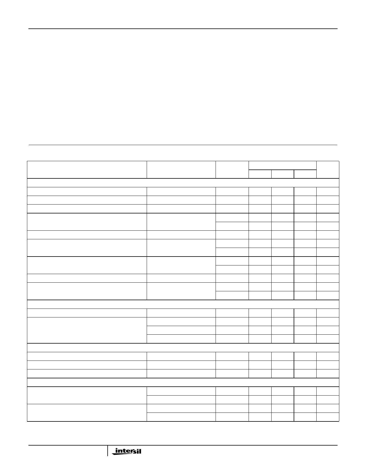
Electrical Specifications VSUPPLY = ±15.0V; CH = Internal = 135pF; Digital Input: VIL = +0.8V (Sample), VIH = +2.0V (Hold). Non-Inverting Unity
Gain Configuration (Output tied to -Input), RL = 2kΩ, CL = 60pF, Unless Otherwise Specified
PARAMETER
TEST CONDITIONS
TEMP. (oC)
HA-5340-5
MIN
TYP
MAX
UNITS
INPUT CHARACTERISTICS
Input Voltage Range
Input Resistance (Note 3)
Input Capacitance
Full
-10
-
+10
V
25
-
1
-
MΩ
25
-
-
3
pF
Input Offset Voltage
25
-
-
1.5
mV
Offset Voltage Temperature Coefficient
Bias Current
Offset Current
Common Mode Range
CMRR
±10V, Note 4
Full
-
-
3.0
mV
Full
-
-
30
µV/oC
25
-
±70
-
nA
Full
-
-
±350
nA
25
-
±50
-
nA
Full
-
-
±350
nA
Full
-10
-
+10
V
25
-
83
-
dB
Full
72
-
-
dB
TRANSFER CHARACTERISTICS
Gain
DC
25
110
140
-
dB
Gain Bandwidth Product
TRANSIENT RESPONSE
Rise Time
CH External = 0pF
CH External = 100pF
CH External = 1000pF
200mV Step
Full
-
10
-
MHz
Full
-
9.6
-
MHz
Full
-
6.7
-
MHz
25
-
20
30
ns
Overshoot
Slew Rate
DIGITAL INPUT CHARACTERISTICS
200mV Step
10V Step
25
-
35
50
%
25
40
60
-
V/µs
Input Voltage
Input Current
VIH
VIL
VIL = 0V
VIH = 5V
Full
2.0
-
-
V
Full
-
-
0.8
V
Full
-
7
40
µA
Full
-
4
40
µA
2
Share Link: 