OR2C08A-7A Ver la hoja de datos (PDF) - Unspecified
Nû¤mero de pieza
componentes Descripciû°n
Fabricante
OR2C08A-7A Datasheet PDF : 192 Pages
| |||
ORCA Series 2 FPGAs
Data Sheet
June 1999
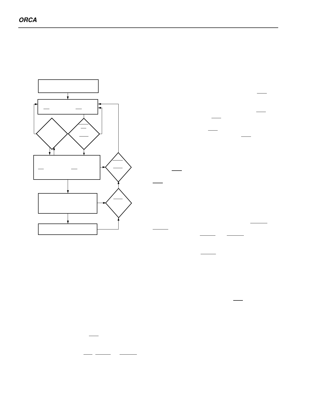
FPGA States of Operation
Prior to becoming operational, the FPGA goes through a
sequence of states, including initialization, configuration,
and start-up. Figure 36 outlines these three FPGA
states.
POWERUP
ã POWER-ON TIME DELAY
INITIALIZATION
ã CLEAR CONFIGURATION MEMORY
ã INIT LOW, HDC HIGH, LDC LOW
BIT
YES
ERROR
NO
RESET,
INIT,
OR
PRGM
LOW
NO
YES
CONFIGURATION
ã M[3:0] MODE IS SELECTED
ã CONFIGURATION DATA FRAME WRITTEN
ã INIT HIGH, HDC HIGH, LDC LOW
ã DOUT ACTIVE
RESET
OR
PRGM
LOW
START-UP
ã ACTIVE I/O
ã RELEASE INTERNAL RESET
ã DONE GOES HIGH
PRGM
LOW
OPERATION
5-4529(F).r6
Figure 36. FPGA States of Operation
Initialization
Upon powerup, the device goes through an initialization
process. First, an internal power-on-reset circuit is trig-
gered when power is applied. When VDD reaches the
voltage at which portions of the FPGA begin to operate
(2.5 V to 3 V for the OR2CxxA, 2.2 V to 2.7 V for the
OR2TxxA/OR2TxxB), the I/Os are configured based on
the configuration mode, as determined by the mode
select inputs M[2:0]. A time-out delay is initiated when
VDD reaches between 3.0 V and 4.0 V (OR2CxxA) or
2.7 V to 3.0 V (OR2TxxA/2TxxB) to allow the power
supply voltage to stabilize. The INIT and DONE outputs
are low. At powerup, if VDD does not rise from 2.0 V to
VDD in less than 25 ms, the user should delay configu-
ration by inputting a low into INIT, PRGM, or RESET
until VDD is greater than the recommended minimum
operating voltage (4.75 V for OR2CxxA commercial
devices and 3.0 V for OR2TxxA/B devices).
At the end of initialization, the default configuration
option is that the configuration RAM is written to a low
state. This prevents shorts prior to configuration. As a
configuration option, after the first configuration (i.e., at
reconfiguration), the user can reconfigure without
clearing the internal configuration RAM first.
The active-low, open-drain initialization signal INIT is
released and must be pulled high by an external resis-
tor when initialization is complete. To synchronize the
configuration of multiple FPGAs, one or more INIT pins
should be wire-ANDed. If INIT is held low by one or
more FPGAs or an external device, the FPGA remains
in the initialization state. INIT can be used to signal that
the FPGAs are not yet initialized. After INIT goes high
for two internal clock cycles, the mode lines (M[3:0])
are sampled and the FPGA enters the configuration
state.
The high during configuration (HDC), low during config-
uration (LDC), and DONE signals are active outputs in
the FPGAãs initialization and configuration states. HDC,
LDC, and DONE can be used to provide control of
external logic signals such as reset, bus enable, or
PROM enable during configuration. For parallel master
configuration modes, these signals provide PROM
enable control and allow the data pins to be shared
with user logic signals.
If configuration has begun, an assertion of RESET or
PRGM initiates an abort, returning the FPGA to the ini-
tialization state. The PRGM and RESET pins must be
pulled back high before the FPGA will enter the config-
uration state. During the start-up and operating states,
only the assertion of PRGM causes a reconfiguration.
In the master configuration modes, the FPGA is the
source of configuration clock (CCLK). In this mode, the
initialization state is extended to ensure that, in daisy-
chain operation, all daisy-chained slave devices are
ready. Independent of differences in clock rates, master
mode devices remain in the initialization state an addi-
tional six internal clock cycles after INIT goes high.
When configuration is initiated, a counter in the FPGA
is set to 0 and begins to count configuration clock
cycles applied to the FPGA. As each configuration data
frame is supplied to the FPGA, it is internally assem-
bled into data words. Each data word is loaded into the
internal configuration memory. The configuration load-
ing process is complete when the internal length count
equals the loaded length count in the length count field,
and the required end of configuration frame is written.
40
Lucent Technologies Inc.
Share Link: 