NCP1601A Ver la hoja de datos (PDF) - ON Semiconductor
Número de pieza
componentes Descripción
Fabricante
NCP1601A Datasheet PDF : 18 Pages
| |||
NCP1601A, NCP1601B
There is an internal capacitance Cosc(int) (36 pF typical)
in the oscillator pin and the oscillator frequency is to
fosc(max) (405 kHz typical) when the Osc pin is opened.
Hence, the oscillator switching frequency can be
formulated in (eq.18) and represented in Figure 38.
36 pF @ 405 kHz
Cosc +
fosc
* 36 pF
(eq.18)
700
600
500
400
300
200
100
0
0
50
100
150
200
f osc , Oscillator Frequency (kHz)
Figure 38. Osc Pin Frequency Setting
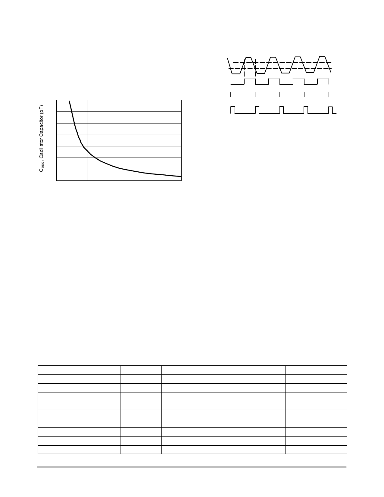
Synchronization Mode
The Osc pin (Pin 5) receives an external digital signal
with level high defined to be higher than Vsync(H) (5 V
typical) and level low defined to be lower than Vsync(L)
(3.5 V typical). An internal 9 V ESD Zener diode is
connected to the Osc pin and hence the maximum
synchronization voltage is 9 V. The circuit recognizes a
synchronization frequency by the time difference between
two falling edge instants when the synchronization signal
across the 3.5 V threshold points. The actual
synchronization threshold point is a slightly higher than the
3.5 V threshold point. The minimum synchronization pulse
width is 500 ns.
There is a typical 350 ns propagation delay from
synchronization threshold point to the moment of output goes
high and there is also a typical 300 ns propagation delay from
the synchronization threshold point to the moment of crossing
3.5 V. Hence, the output goes high apparently when the sync
signal turns to 3.5 V. A timing diagram of synchronization
mode is summarized in Figure 39.
Sync Signal
Osc Clock
Clock Edge
5V
3.5 V
Drive Output
(DCM)
Figure 39. Synchronization Mode Timing Diagram in
DCM
VCC Undervoltage Lockout (UVLO)
There are two UVLO options. The device typically starts
to operate when the supply voltage VCC exceeds 13.75 V
for NCP1601A and 10.5 V for NCP1601B. It turns off when
the supply voltage VCC goes below 9 V. An 18 V internal
ESD Zener diode is connected to the VCC pin (Pin 8).
Hence, the operating range is 9 V to 18 V.
The 4.75 V UVLO hysteresis option of the NCP1601A
and 14 mA low startup current make the self−supply design
easier. The 1.5 V UVLO hysteresis option of NCP1601B
makes it more flexible to match with the second−stage
PWM controller biasing VCC supply voltage.
Thermal Shutdown
An internal thermal circuitry disables the circuit gate
drive and then keeps the power switch off when the junction
temperature exceeds 140°C. The output stage is then
enabled once the temperature drops below typically 95°C
(i.e., 45°C hysteresis). The thermal shutdown is provided
to prevent possible device failures that could result from an
accidental overheating.
Output Drive
The output stage of the device is designed for direct drive
of power MOSFET. It is capable of up to −500 mA and
+750 mA peak drive current and has a typical rise and fall
time of 53 and 32 ns with a 1.0 nF load.
Table 1. Power Factor Controller Test Data
Vin (Vac)
90
Pin (W)
143.4
Vout (V)
327
110
161.1
373
130
160.5
378
150
160.9
382
180
161.6
386
190
161.7
387
210
162.0
389
230
162.2
391
250
162.8
393
Iout (mA)
400
400
400
400
400
400
400
400
400
PF
0.998
0.997
0.996
0.993
0.990
0.986
0.980
0.973
0.959
THD (%)
4
6
6
7
6
8
8
9
16
Efficiency (%)
91.2
92.6
94.2
95.0
95.5
95.7
96.0
96.4
96.6
http://onsemi.com
14
Share Link: 