MPC7457(2004) Ver la hoja de datos (PDF) - Freescale Semiconductor
Número de pieza
componentes Descripción
Fabricante
MPC7457 Datasheet PDF : 68 Pages
| |||
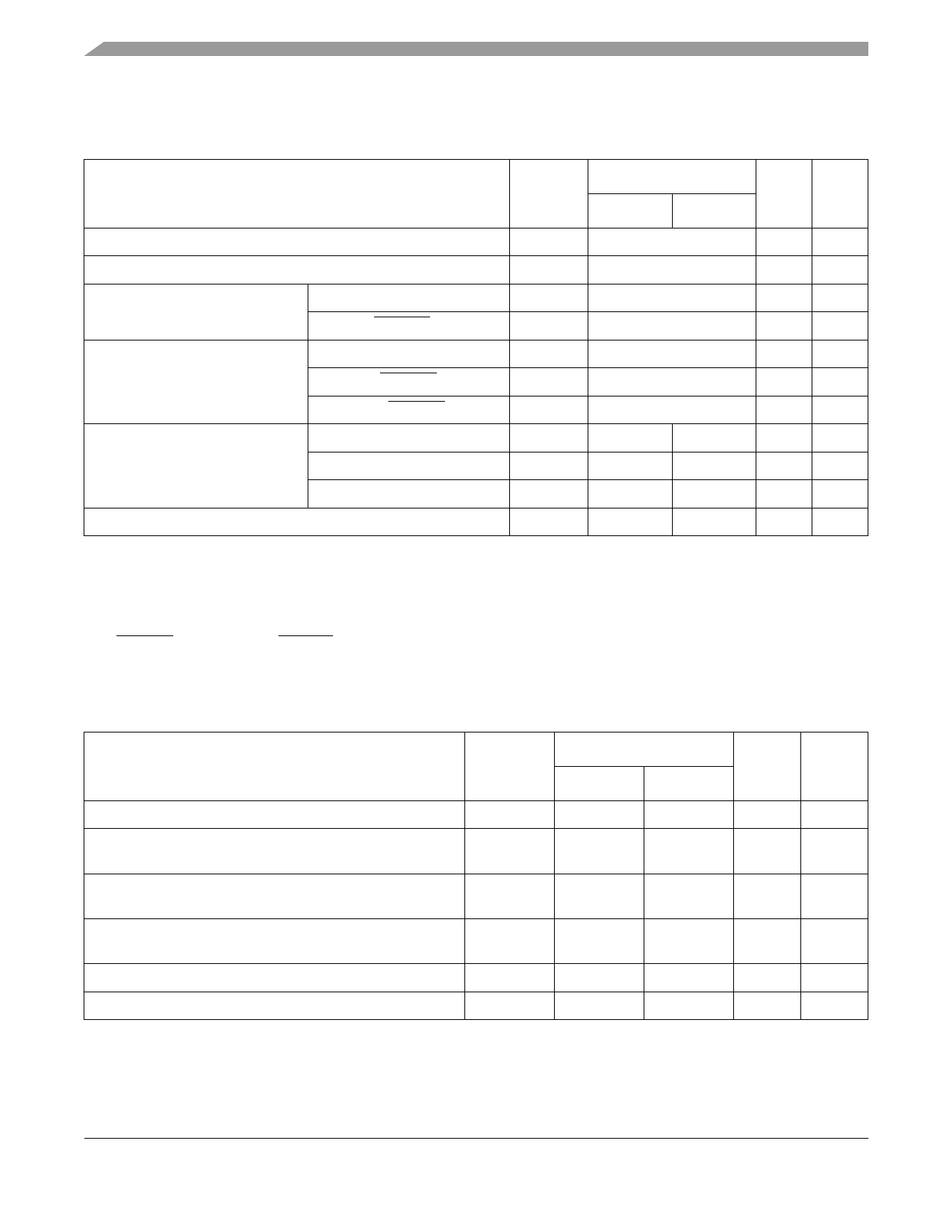
Electrical and Thermal Characteristics
Table 6. DC Electrical Specifications (continued)
At recommended operating conditions. See Table 4.
Characteristic
Nominal
Bus Symbol
Min
Voltage 1
Max
Unit Notes
Output high voltage, IOH = –5 mA
1.5
VOH OVDD/GVDD – 0.45
—
1.8
OVDD/GVDD – 0.45
—
2.5
1.8
—
V
6
V
V
Output low voltage, IOL = 5 mA
1.5
VOL
—
1.8
—
0.45
V
6
0.45
V
2.5
—
0.6
V
Capacitance,
L3 interface
—
Cin
—
Vin = 0 V, f = 1 MHz All other inputs
—
9.5
pF
5
8.0
Notes:
1. Nominal voltages; see Table 4 for recommended operating conditions.
2. For processor bus signals, the reference is OVDD while GVDD is the reference for the L3 bus signals.
3. Excludes test signals and IEEE 1149.1 boundary scan (JTAG) signals.
4. The leakage is measured for nominal OVDD/GVDD and VDD, or both OVDD/GVDD and VDD must vary in the same direction
(for example, both OVDD and VDD vary by either +5% or –5%).
5. Capacitance is periodically sampled rather than 100% tested.
6. Applicable to L3 bus interface only.
Table 7 provides the power consumption for the MPC7457.
Table 7. Power Consumption for MPC7457
Processor (CPU) Frequency
867 MHz
1000 MHz
1200 MHz
1267 MHz
Typical
Maximum
Typical
Typical
Full-Power Mode
14.8
15.8
17.5
18.3
21.0
22.0
24.2
25.6
Nap Mode
5.2
5.2
5.2
5.2
Sleep Mode
5.1
5.1
5.1
5.1
Unit Notes
W
1, 2
W
1, 3
W
1, 2
W
1, 2
MPC7457 RISC Microprocessor Hardware Specifications, Rev. 5
14
Freescale Semiconductor
Share Link: 