MCP3909T Ver la hoja de datos (PDF) - Microchip Technology
Número de pieza
componentes Descripción
Fabricante
MCP3909T Datasheet PDF : 44 Pages
| |||
MCP3909
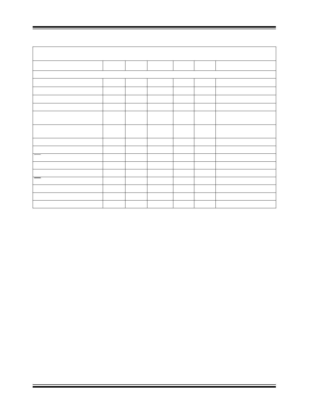
TIMING CHARACTERISTICS (CONTINUED)
Electrical Specifications: Unless otherwise indicated, all parameters apply at AVDD = DVDD = 4.5V to 5.5V,
AGND, DGND = 0V, MCLK = 3.58 MHz; TA = -40°C to +85°C.
Parameter
Sym
Min
Typ
Max Units
Comment
Serial Interface Timings (Note 4)
Data Ready Pulse Width
Reset Time
Output Data Rate
Serial Clock Frequency
Window for serial mode entry
codes
tDR
4/MCLK
tRST
100
—
—
fADC
— MCLK/256 —
fCLK
—
20
tWINDOW
—
—
32/
MCLK
ns
MHz
—
VDD = 5V
Last bit must be clocked in
before this time.
Window start time for serial
mode entry codes
tWINSET 1/MCLK
—
—
— First bit must be clocked in
after this time.
Serial Clock High Time
tHI
—
—
25
ns fCLK= 20 MHz
Serial Clock Low Time
tLO
—
—
25
ns fCLK= 20 MHz
CS Fall to First Rising CLK Edge tSUCS
15
—
—
ns
Data Input Setup Time
tSU
10
—
—
ns
Data Input Hold Time
tHD
—
—
10
ns
CS Rise to Output Disable
tDIS
—
—
150
ns
CLK Rise to Output Data Valid
tDO
—
—
30
ns
SDO Rise Time
tR
—
2
—
ns
SDO Fall Time
tF
—
2
—
ns
Note 1:
2:
3:
If output pulse period (tFP) falls below 984376*2 MCLK periods, then tFW = 1/2 tFP.
If output pulse period (tHP) falls below 322160*2 MCLK periods, then tHW = 1/2 tHP. When F2, F1, F0
equals 0,1,1, the HFOUT pulse time is fixed at 64 x MCLK periods or 18 µs for MCLK = 3.58 MHz.
Specified by characterization, not production tested.
4: Serial timings specified and production tested with 180 pF load.
DS22025C-page 6
2006-2012 Microchip Technology Inc.
Share Link: 