LC9947G Ver la hoja de datos (PDF) - SANYO -> Panasonic
Número de pieza
componentes Descripción
Fabricante
LC9947G Datasheet PDF : 9 Pages
| |||
LC9947G
Clock Voltage at frame shift frequency = 3.58 MHz
Parameter
Symbol
Conditions
Imaging block pulses: ø1, ø2, ø3, ø4
Pulse amplitude
Low level
Storage block pulses: øS1, øS2
VPIF
*
VLIF
*
Pulse amplitude
Low level
Storage block pulses: øS3, øS4
VPSL
VLSL
Pulse amplitude
Low level
Horizontal transfer pulses: øH1, øH2
VPSL
VLSL
Pulse amplitude
VPH
Low level
VLH
Reset gate: øR
Pulse amplitude
VPR
Low level
VLR
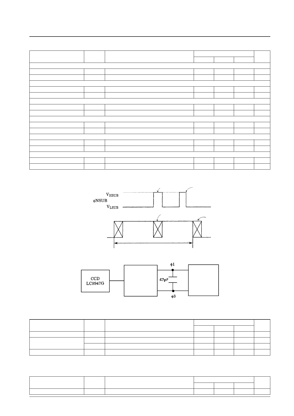
Substrate pulse: øNSUB
High level
VHSUB** See Figure 1
Low level
VLSUB See Figure 1
Note: * A 47 pF capacitor must be inserted as shown in figure 2.
** Adjust the VHNS saturation output to its maximum value without causing picture degradation.
Ratings
Unit
min
typ
max
14.0
14.5
15.0
V
–10.0
–9.5
–9.0
V
14.0
14.5
15.0
V
–7.0
–6.5
–6.0
V
14.0
14.5
15.0
V
–8.0
–7.5
–7.0
V
4.5
5.0
5.5
V
0
0
0.5
V
4.5
5.0
5.5
V
3.6
4.0
4.4
V
30.0
40.0
V
17.5
18.0
18.5
V
Shutter pulse
Slice pulse
Imaging area pulse
Charge sweep pulse
Frame
shift
One field
Fig. 1
Vertical driver
IC
LB89901V
Timing
IC
LC99012A
Bias Conditions
Fig. 2
Parameter
Symbol
Conditions
P-well
VPW
Output circuit voltage
OG bias
VDD
*1
VGG
*2
VOG
*2
Note: 1. This level must not become higher than the substrate pulse low level VLSUB.
2. These input pins are in high impedance state.
DC Characteristics
Parameter
DC operating current
Symbol
IDD
Conditions
Ratings
Unit
min
typ
max
0
V
14.5
15.0
15.5
V
0.5
0.8
1.1
V
4.5
5.0
5.5
V
Ratings
Unit
min
typ
max
2.5
4.5
6.5
mA
No. 4971-4/9
Share Link: 