MF3129-J8CATXX Ver la hoja de datos (PDF) - MITSUBISHI ELECTRIC
Número de pieza
componentes Descripción
Fabricante
MF3129-J8CATXX Datasheet PDF : 16 Pages
| |||
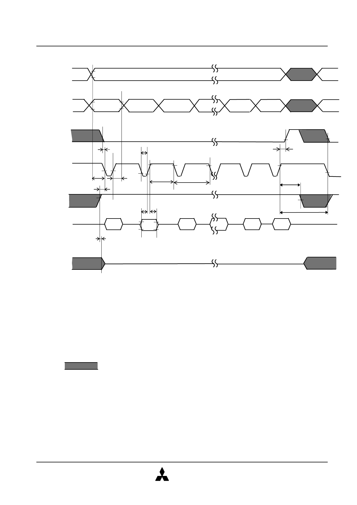
PAGE MODE WRITE TIMING CHART
An=(n>5)
MITSUBISHI MEMORY CARD
STATIC RAM CARDS
An
(A0~A5)
0h
2h
4h
3Ch
3Eh
CE#
tsu(CE)R
tw(WE)R
WE#
tsu(A)R
tsu(OE-WE)R
OE#
DIN Hi-Z
tdis(OE)R
tDLR
trec(WE)R
tBLCR
t(D-WEH)R
th(D)R
DOUT
Hi-Z
th(CE)R
th(OE-WE)R
tcWR
REG#=“L” level
Note 6 : Test Conditions
Input pulse levels
: VIL=0.4V, VIH=2.8V
Input pulse rise, fall time : tr=tf=10ns
Reference voltage
Input
: VIL=0.8V, VIH=2.4V
Output
: VOL=0.8V, VOH=2.0V
(ten and tdis are measured when output voltage is ± 500mV from steady state. )
Load
: 100pF + 1 TTL gate
5pF + 1 TTL gate (at ten and tdis measuring)
7:
Indicates the don’t care input
8 : Writing is executed in overlap of CE# and WE# are “L” level. (only for Common Memory)
9 : Don’t apply inverted phase signal externally when Dm pin is in output mode.
10 : CE# is indicated as follows:
Read A/Write A : CE#=CE1#=CE2#
Read B/Write B : CE#=CE1#, CE2#=“H” level
Read C/Write C : CE#=CE2#, CE1#=“H” level
MITSUBISHI
ELECTRIC
12/16
Apr. 1999 Rev. 1.2
Share Link: 