M24C64-DFBN6G Ver la hoja de datos (PDF) - STMicroelectronics
NГәmero de pieza
componentes DescripciГіn
Fabricante
M24C64-DFBN6G Datasheet PDF : 45 Pages
| |||
DC and AC parameters
M24C64-W M24C64-R M24C64-F
Table 9. AC measurement conditions
Symbol
Parameter
Min.
Max.
Unit
Cbus Load capacitance
100
pF
-
SCL input rise/fall time, SDA input fall time
-
50
ns
-
Input levels
0.2 VCC to 0.8 VCC
V
-
Input and output timing reference levels
0.3 VCC to 0.7 VCC
V
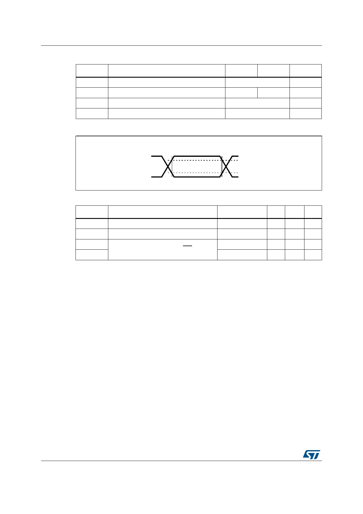
Figure 13. AC measurement I/O waveform
)NPUT�VOLTAGE�LEVELS
6##
6##
)NPUT�AND�OUTPUT
4IMING�REFERENCE�LEVELS
6##
6##
-36
Symbol
Table 10. Input parameters
Parameter(1)
Test condition
CIN
Input capacitance (SDA)
-
CIN
Input capacitance (other pins)
-
ZL
Input impedance (E2, E1, E0, WC)(2)
ZH
VIN < 0.3 VCC
VIN > 0.7 VCC
1. Characterized only, not tested in production.
2. E2, E1, E0 input impedance when the memory is selected (after a Start condition).
Min. Max. Unit
-
8
pF
-
6
pF
30
-
kО©
500 -
kО©
24/45
DocID16891 Rev 30
Share Link: 