LT5521 Ver la hoja de datos (PDF) - Linear Technology
Número de pieza
componentes Descripción
Fabricante
LT5521 Datasheet PDF : 16 Pages
| |||
LT5521
APPLICATIO S I FOR ATIO
3.5
30
2.5
TA = 25°C
1.5
fIF = 250MHz
fLO = 1.7GHz
fRF = 1.95GHz
0.5
IIP3
25
20
15
NF
–0.5
10
GC
–1.5
5
–2.5
0 20
40 60 80 100
R1 AND R7 (Ω)
0
120 140
5521 F06
Figure 6. IIP3, GC and Noise Figure vs External Resistance,
Constant Core Current (Variable Supply Voltage)
1.8
TA = 25°C
fIF = 250MHz
1.2 fLO = 1.7GHz
fRF = 1.95GHz
0.6 VCC = 4V
30
25
IIP3
20
0
15
NF
–0.6
10
–1.2
GC
5
–1.8
15
0
20 25 30 35 40 45
CORE CURRENT (mA)
5521 F07
Figure 7. IIP3, GC and Noise Figure vs Core Current,
Constant Supply Voltage
9
7
TA = 25°C fRF = 1.95GHz
5 fIF = 250MHz VCC = 3.3V
fLO = 1.7GHz
3
RFC
1
GC
RFC
–1
30
IIP3
25
RFC
20
NF
15
10
5
–3
0
25 30 35 40 45 50 55
CORE CURRENT (mA)
5521 F08
Figure 8. Comparison of 3.3V Performance With
and Without Input RF Choke
12
The user can tailor the biasing of the LT5521 to meet
individual system requirements. It is recommended to
choose a source resistance as large as possible to mini-
mize sensitivity to power supply variation.
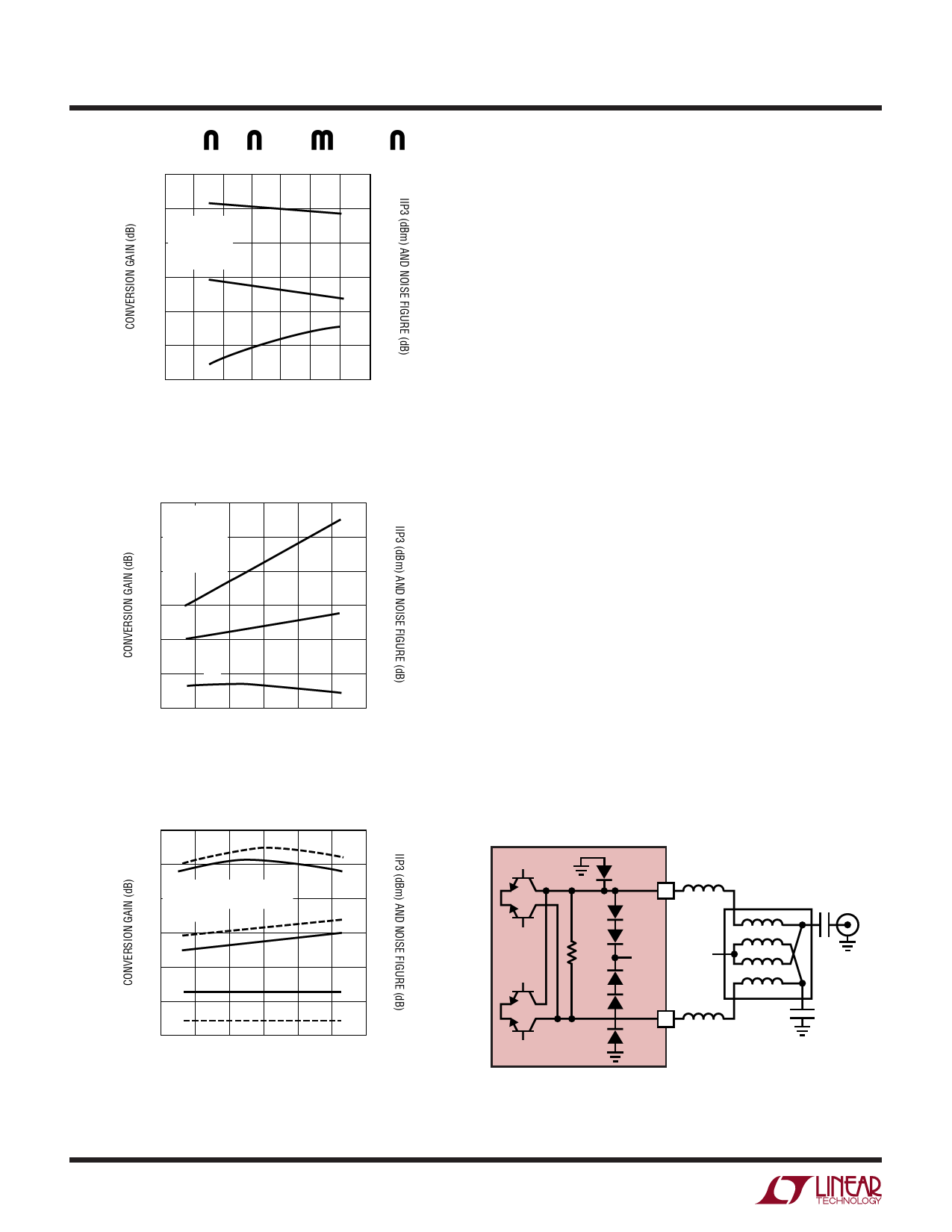
Output Interface
A DC connection to VCC must be provided on the PCB to the
output pins. These pins will draw approximately 20mA
each from the power supply. On-chip, there is a nominal
300Ω differential resistance between the output pins.
Figure 9 shows a typical matching circuit using an external
balun to provide differential to single-ended conversion.
LO suppression and 2xLO suppression are influenced by
the symmetry of the external output matching circuitry.
PCB design must maintain the trace layout symmetry of
the output pins as much as possible to minimize these
signals.
The M/A-COM ETC1.6-4-2-3 4:1 transformer (T2, Fig-
ure␣ 9) is suitable for applications with output frequencies
between 500MHz and 2700MHz. Output matching at vari-
ous frequencies is achieved by adding inductors in series
with the output (L1, L2) and DC blocking capacitor C3, as
shown in Figure 9. Table 6 specifies center frequency and
bandwidth of the output match for different matching
configurations. Figure 10 shows the typical output return
loss vs frequency for 1GHz and 2GHz applications. Capaci-
tor C12 provides a solid AC ground at the RF output
frequency.
LT5521
OUT+
L1
12
300Ω
VCC
VCC
OUT–
L2
9
T2
4:1
C3
OUT
C12
5521 F09
Figure 9. Simplified Output Circuit
with External Matching Components
5521f
Share Link: 