LT1375 Ver la hoja de datos (PDF) - Linear Technology
Número de pieza
componentes Descripción
Fabricante
LT1375 Datasheet PDF : 28 Pages
| |||
LT1375/LT1376
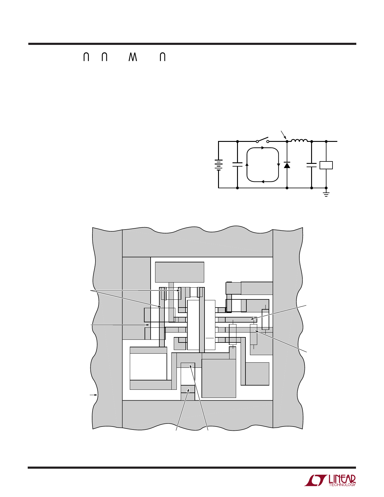
APPLICATIONS INFORMATION
(magnetic) radiation is minimized by keeping catch diode,
switch pin, and input bypass capacitor leads as short as
possible. E field radiation is kept low by minimizing the
length and area of all traces connected to the switch pin
and BOOST pin. A ground plane should always be used
under the switcher circuitry to prevent interplane cou-
pling. A suggested layout for the critical components is
shown in Figure 5. Note that the feedback resistors and
compensation components are kept as far as possible
from the switch node. Also note that the high current
ground path of the catch diode and input capacitor are kept
very short and separate from the analog ground line.
The high speed switching current path is shown schemati-
cally in Figure 6. Minimum lead length in this path is
essential to ensure clean switching and low EMI. The path
including the switch, catch diode, and input capacitor is
the only one containing nanosecond rise and fall times. If
you follow this path on the PC layout, you will see that it is
irreducibly short. If you move the diode or input capacitor
away from the LT1376, get your resumé in order. The
other paths contain only some combination of DC and
500kHz triwave, so are much less critical.
SWITCH NODE
L1
5V
HIGH
FREQUENCY
VIN
CIRCULATING
PATH
LOAD
Figure 6. High Speed Switching Path
1375/76 F06
MINIMIZE AREA OF
CONNECTIONS TO THE
SWITCH NODE AND
BOOST NODE
KEEP INPUT CAPACITOR
AND CATCH DIODE CLOSE
TO REGULATOR AND
TERMINATE THEM
TO SAME POINT
GROUND RING NEED
NOT BE AS SHOWN.
(NORMALLY EXISTS AS
INTERNAL PLANE)
16
INPUT
C2
D2
BOOST
VC
C3
IN
FB
SW
GND
D1
BIAS
SHDN
CC
RC
R1
R2
L1
C1
OUTPUT
SHUTDOWN
MINIMIZE SIZE OF
FEEDBACK PIN
CONNECTIONS TO
AVOID PICKUP
TERMINATE
FEEDBACK RESISTORS
AND COMPENSATION
COMPONENTS
DIRECTLY TO SWITCHER
GROUND PIN
CONNECT OUTPUT CAPACITOR
DIRECTLY TO HEAVY GROUND
TAKE OUTPUT DIRECTLY FROM END OF OUTPUT
CAPACITOR TO AVOID PARASITIC RESISTANCE
AND INDUCTANCE (KELVIN CONNECTION)
Figure 5. Suggested Layout
1375/76 F05
Share Link: 