LC75836W Ver la hoja de datos (PDF) - SANYO -> Panasonic
Número de pieza
componentes Descripción
Fabricante
LC75836W Datasheet PDF : 18 Pages
| |||
LC75836W
Notes on Controller Transfer of Display Data
Since the LC75836W transfer the display data (D1 to D140) in four separate transfer operations, we recommend that
applications make a point of completing all four data transfers within a period of less than 30ms to prevent
observable degradation of display quality.
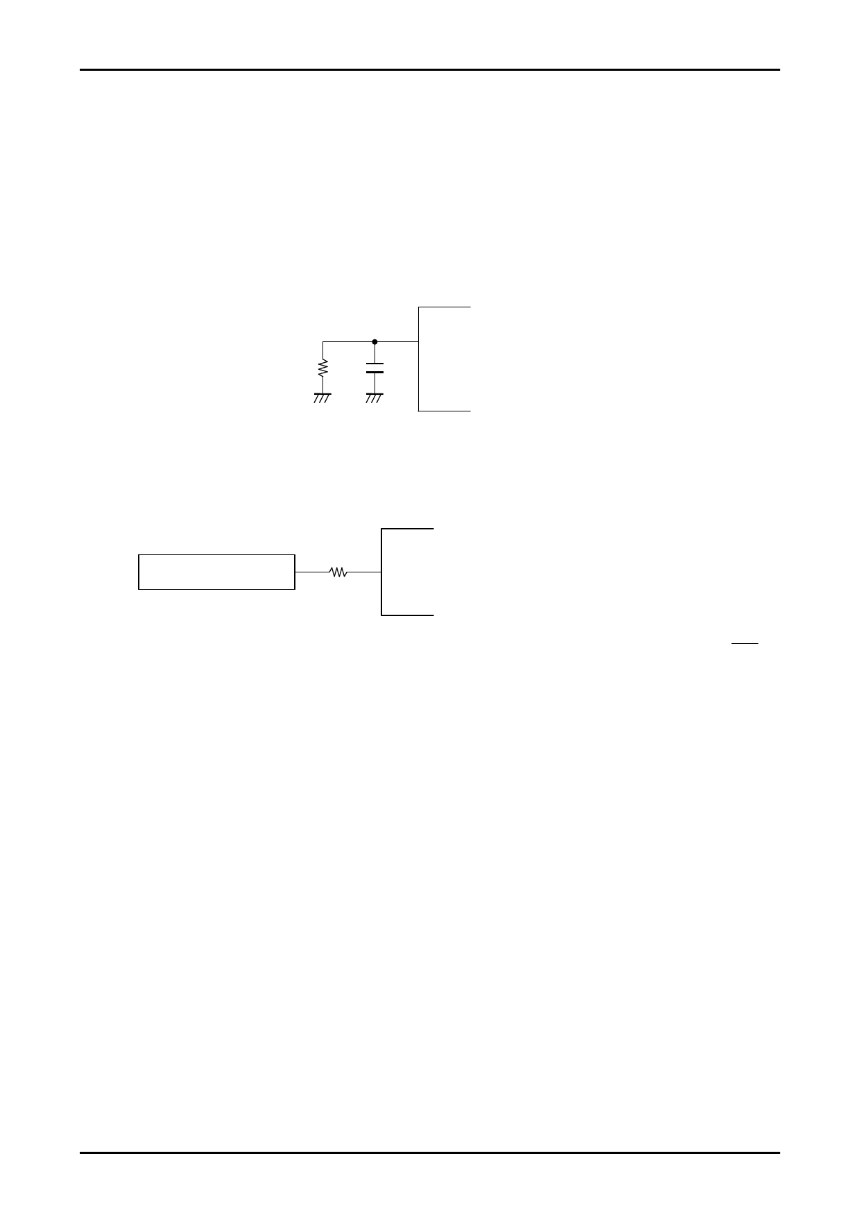
OSC Pin Peripheral Circuit
(1) RC oscillator operating mode (control data OC = 0)
An external resistor, Rosc, and an external capacitor, Cosc, must be connected between the OSC pin and GND if
RC oscillator operating mode is selected.
Rosc
OSC
Cosc
(2) External clock operating mode (control data OC = 1)
When the external clock operating mode is selected, insert a current protection resistor Rg (4.7 to 47kΩ) between
the OSC pin and external clock output pin (external oscillator). Determine the value of the resistance according to
the allowable current value at the external clock output pin. Also make sure that the waveform of the external
clock is not heavily distorted.
External clock output pin
Rg
External oscillator
OSC
Note: Allowable current value at external clock output pin > VDD
Rg
No.A0428-16/18
Share Link: 