LB1951 Ver la hoja de datos (PDF) - SANYO -> Panasonic
Número de pieza
componentes Descripción
Fabricante
LB1951 Datasheet PDF : 9 Pages
| |||
LB1951V
Continued from preceding page.
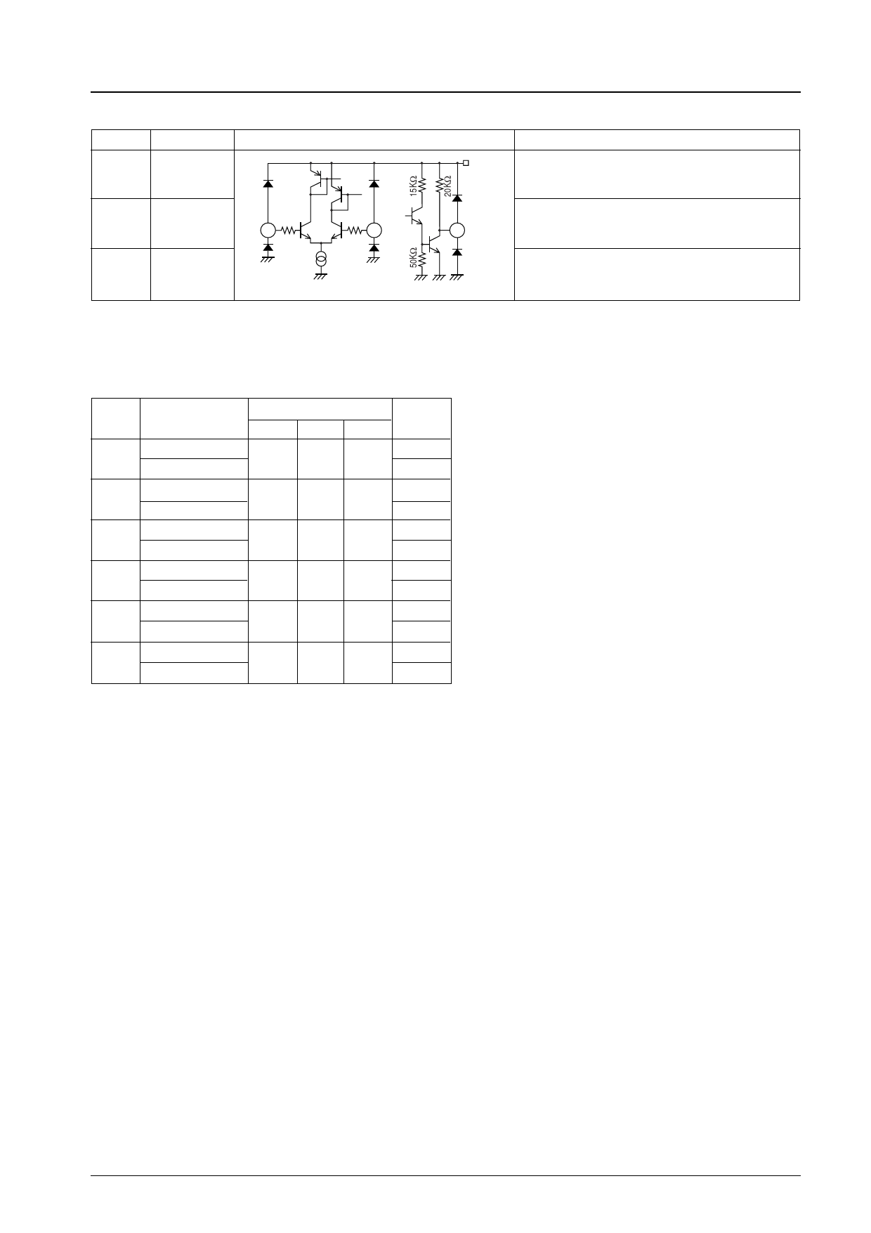
Pin No. Pin name
22
FGIN+
I/O equivalent circuit
VCC1
23
FGIN–
24
FGOUT
FGIN—
23
200Ω
FGIN+
22
200Ω
24 FGOUT
A12472
Function
Noninverting input pin for the FG comparator.
No bias is applied internally.
Inverting input pin for the FG comparator.
No bias is applied internally.
FG comparator output pin. A resistive load of 20 kΩ
is provided internally.
Truth Table
Source → Sink
V→W
1
W →V
U →W
2
W→U
U→V
3
V→U
W →V
4
V→W
W→U
5
U →W
V→U
6
U→V
Hall input
U
V
W
H
H
L
H
L
L
H
L
H
L
L
H
L
H
H
L
H
L
FRC
H
L
H
L
H
L
H
L
H
L
H
L
Note: ‘‘H’’ in the FRC column represents a voltage of 2.5 V or
more; ‘‘L’’ represents a voltage of 0.4 V or less.
(At VCC1 =3 V)
Note: ‘‘H’’ in the Hall input columns represents a state in
which ‘‘+’’ has a potential which is higher by 0.02 V or
more than that of the ‘‘–’’ phase inputs.
Conversely, ‘‘L’’ represents a state in which ‘‘+’’ has a
potential which is lower by 0.02 V or more than that of
the ‘‘–’’ phase input.
No. 5232-5/9
Share Link: 