L6563 Ver la hoja de datos (PDF) - STMicroelectronics
Número de pieza
componentes Descripción
Fabricante
L6563 Datasheet PDF : 37 Pages
| |||
L6563 - L6563A
Application information
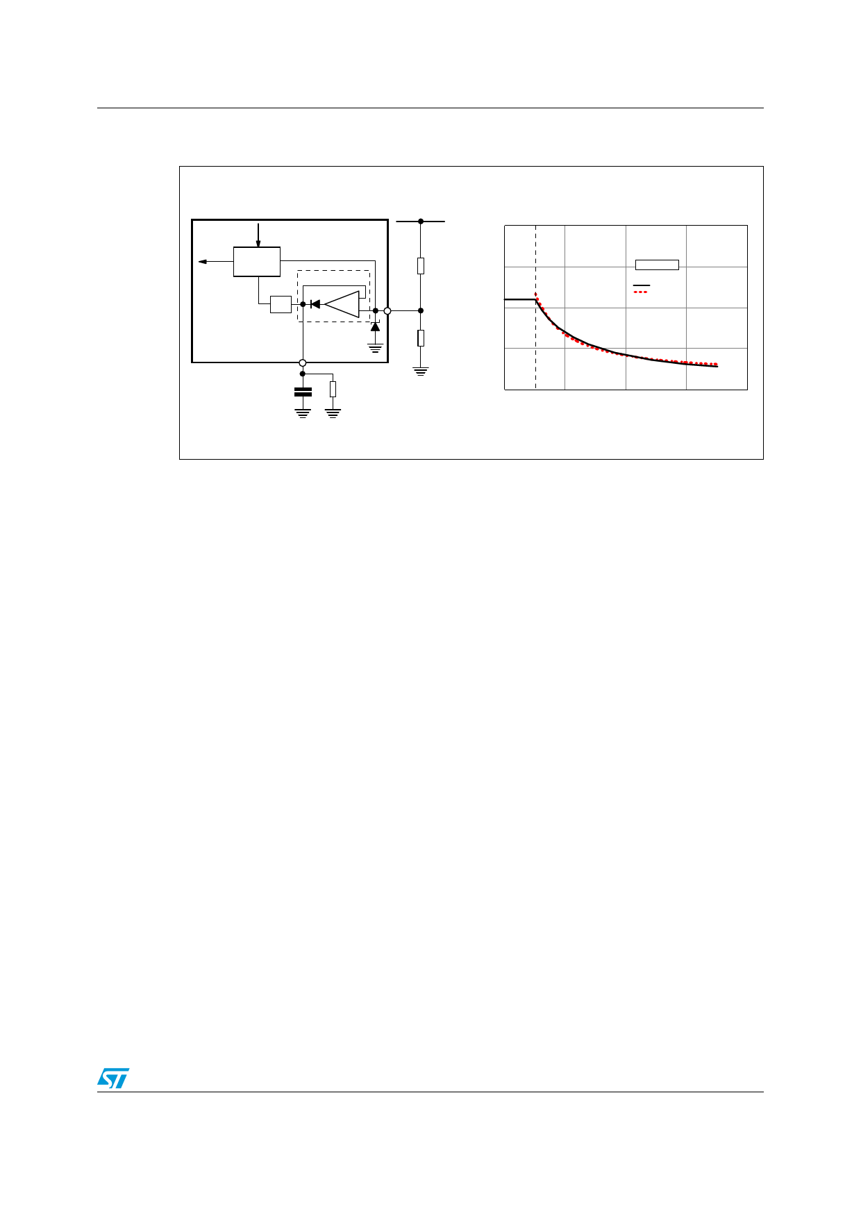
Figure 34. Voltage feedforward: squarer-divider (1/V2) block diagram and transfer
characteristic
Rectified mains
current
ref erence
E/A output
(VCOMP)
(Vcsx)
MULTIPLIER
R5
"ideal" diode
L6563
L6563A
1/V 2
5
-
+
9.5V
3
MULT
R6
Vcsx
2
1.5
1
0.5
VCOMP=4V
Actual
Ideal
VFF
CFF
RFF
0
0 0.5
1
2
3
4
VFF=VMULT
In this way a change of the line voltage will cause an inversely proportional change of the
half sine amplitude at the output of the multiplier (if the line voltage doubles the amplitude of
the multiplier output will be halved and vice versa) so that the current reference is adapted to
the new operating conditions with (ideally) no need for invoking the slow dynamics of the
error amplifier. Additionally, the loop gain will be constant throughout the input voltage
range, which improves significantly dynamic behavior at low line and simplifies loop design.
Actually, deriving a voltage proportional to the RMS line voltage implies a form of integration,
which has its own time constant. If it is too small the voltage generated will be affected by a
considerable amount of ripple at twice the mains frequency that will cause distortion of the
current reference (resulting in high THD and poor PF); if it is too large there will be a
considerable delay in setting the right amount of feedforward, resulting in excessive
overshoot and undershoot of the pre-regulator's output voltage in response to large line
voltage changes. Clearly a trade-off is required.
The device realizes Voltage Feedforward with a technique that makes use of just two
external parts and that limits the feedforward time constant trade-off issue to only one
direction. A capacitor CFF and a resistor RFF , both connected from the VFF (pin 5) pin to
ground, complete an internal peak-holding circuit that provides a DC voltage equal to the
peak of the rectified sine wave applied on pin MULT (pin 3). RFF provides a means to
discharge CFF when the line voltage decreases (see Figure 34). In this way, in case of
sudden line voltage rise, CFF will be rapidly charged through the low impedance of the
internal diode and no appreciable overshoot will be visible at the pre-regulator's output; in
case of line voltage drop CFF will be discharged with the time constant RFF·CFF, which can
be in the hundred ms to achieve an acceptably low steady-state ripple and have low current
distortion; consequently the output voltage can experience a considerable undershoot, like
in systems with no feedforward compensation.
19/37
Share Link: 