L6562A Ver la hoja de datos (PDF) - STMicroelectronics
Número de pieza
componentes Descripción
Fabricante
L6562A Datasheet PDF : 26 Pages
| |||
Application information
L6562A
7.4
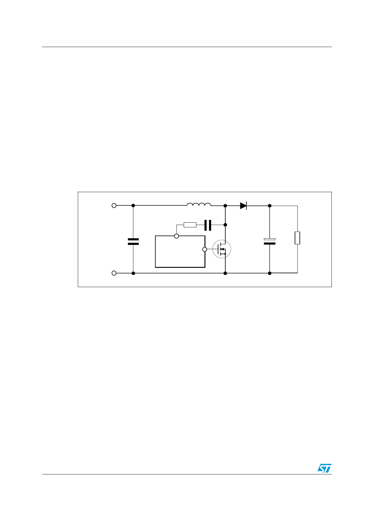
Operating with no auxiliary winding on the boost inductor
To generate the synchronization signal on the ZCD pin, the typical approach requires the
connection between the pin and an auxiliary winding of the boost inductor through a limiting
resistor. When the device is supplied by the cascaded DC-DC converter, it is necessary to
introduce a supplementary winding to the PFC choke just to operate the ZCD pin.
Another solution could be implemented by simply connecting the ZCD pin to the drain of the
power MOSFET through an R-C network as shown in figure 3: in this way the high-
frequency edges experienced by the drain will be transferred to the ZCD pin, hence arming
and triggering the ZCD comparator.
Also in this case the resistance value must be properly chosen to limit the current
sourced/sunk by the ZCD pin. In typical applications with output voltages around 400V,
recommended values for these components are 22pF (or 33pF) for CZCD and 330k for
RZCD. With these values proper operation is guaranteed even with few volts difference
between the regulated output voltage and the peak input voltage
Figure 20. ZCD pin synchronization without auxiliary winding
RZCD CZCD
ZCD
5
L6562A
16/26
Share Link: 