IS25LD256C Ver la hoja de datos (PDF) - Integrated Silicon Solution
Número de pieza
componentes Descripción
Fabricante
IS25LD256C
Integrated Silicon Solution

IS25LD256C Datasheet PDF : 33 Pages
| |||
IS25LD256C
DEVICE OPERATION (CONTINUED)
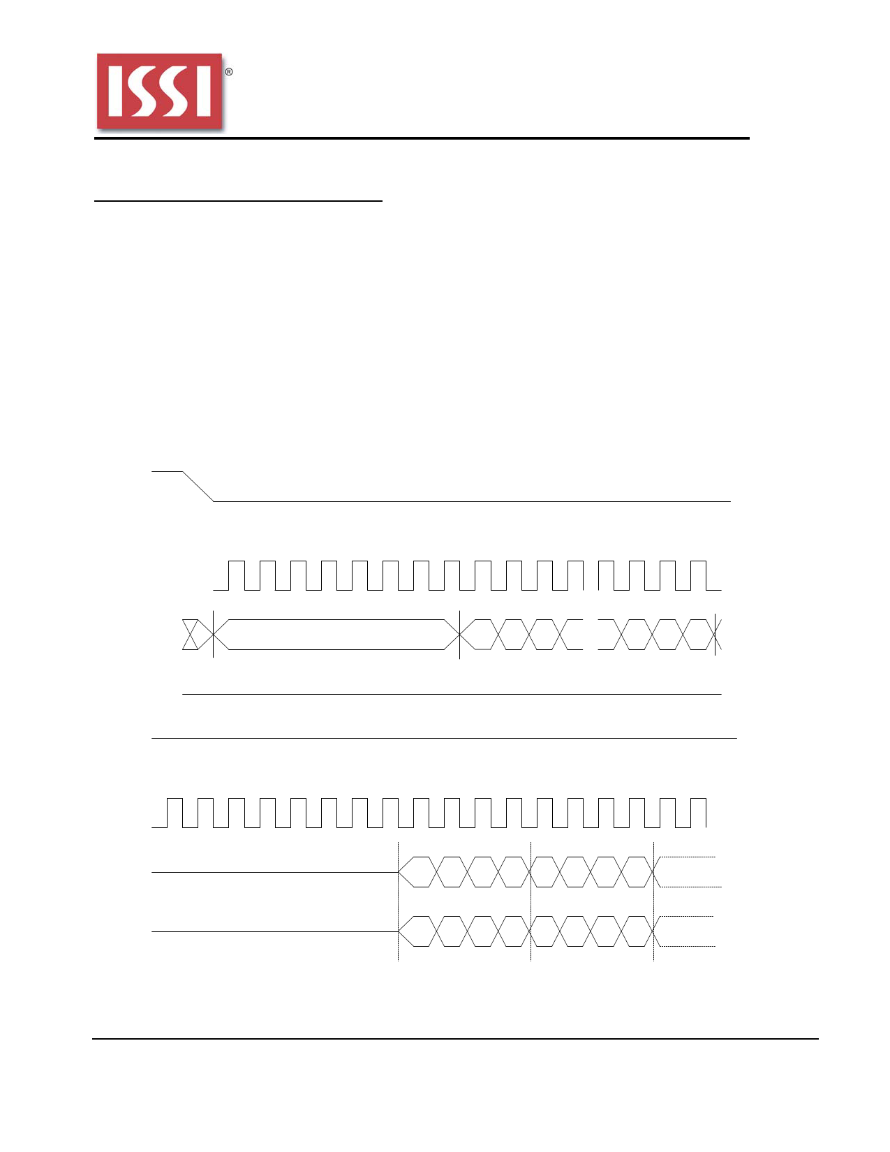
FRDO COMMAND (FAST READ DUAL OUTPUT) OPERATION
The FRDO instruction is used to read memory data on is output on SO, while simultaneously the second bit is
two output pins each at up to a 100 MHz clock.
output on SIO.
The FRDO instruction code is followed by three
The first byte addressed can be at any memory
address bytes (A23 - A0) and a dummy byte (8 clocks), location. The address is automatically incremented
transmitted via the SI line, with each bit latched-in
after each byte of data is shifted out. When the highest
during the rising edge of SCK. Then the first data byte address is reached, the address counter will roll over to
addressed is shifted out on the SO and SIO lines, with the 000000h address, allowing the entire memory to be
each pair of bits shifted out at a maximum frequency read with a single FRDO instruction. FRDO instruction
fCT, during the falling edge of SCK. The first bit (MSb) is terminated by driving CE# high (VIH).
Figure 14. Fast Read Dual-Output Sequence
CE#
SCK
SIO
0 1 2 3 4 5 6 7 8 9 10 11 28 29 30 31
...
INSTRUCTION = 0011 1011b
3 - BYTE ADDRESS
23 22 21
... 3 2 1 0
SO
CE#
HIGH IMPEDANCE
32 33 34 35 36 37 38 39 40 41 42 43 44 45 46 47 48
SCK
SIO
SO
HIGH IMPEDANCE
6 42 06 42 06
DATA OUT 1
DATA OUT 2
7 53 17 5 317
Integrated Silicon Solution, Inc.- www.issi.com
19
Rev. A
09/11/2012
Share Link: