UPD75P048GC-AB8 Ver la hoja de datos (PDF) - NEC => Renesas Technology
Número de pieza
componentes Descripción
Fabricante
UPD75P048GC-AB8 Datasheet PDF : 40 Pages
| |||
µPD75P048
3. PROM (PROGRAM MEMORY) WRITE AND VERIFY
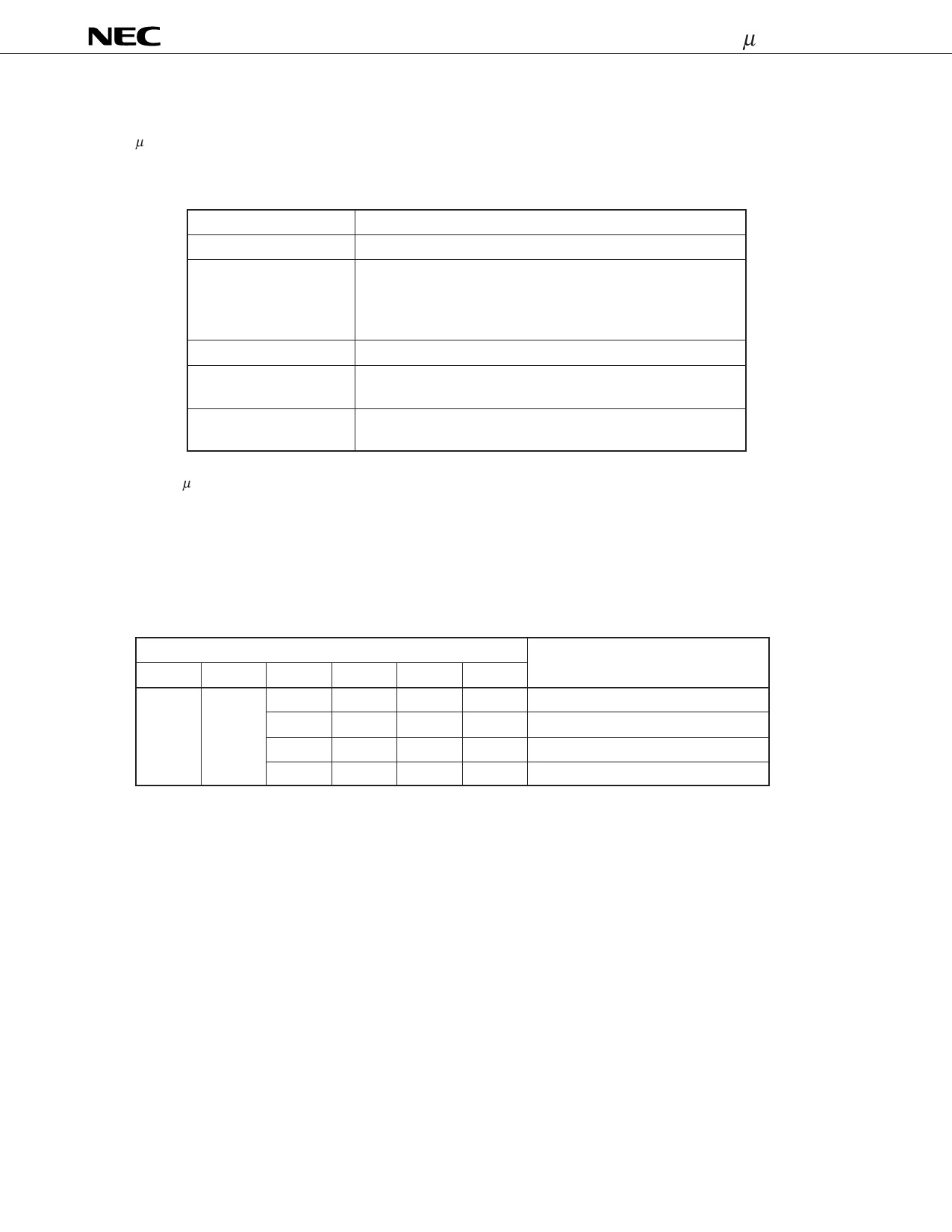
The µPD75P048 contains 8064 bytes of PROM. The following table shows the pin functions during the write
and verify cycles. Note that it is not necessary to enter an address, because the address is updated by pulsing
the X1 clock pins.
Pin Name
VPP
X1, X2
MD0 - MD3 (P30 - P33)
P40 - P43 (lower 4 bits)
P50 - P53 (higher 4 bits)
VDD
Function
Normally 2.7 to 6 V; 12.5 V is applied during write/verify
After a write/verify write, the X1 and X2 clock pins are
pulsed. The inverted signal of the X1 should be input to the
X2.
Note that these pins are also pulsed during a read.
Operation mode selection pins.
8-bit data input/output pins for write and verify
Supply voltage.
Normally 2.7 to 6 V; 6 V is applied during write/verify
Caution The µPD75P048CW/GC do not have a UV erase window, thus the PROM contents cannot be erased
with ultra-violet ray.
3.1 PROM WRITE AND VERIFY OPERATION MODE
When 6 V and 12.5 V are applied to the VDD and VPP pins, respectively, the PROM is placed in the write/verify
mode. The operation is selected by the MD0 to MD3 pins, as shown in the table.
The other pins should be returned to VSS potential via pull-down resistors.
VPP
+12.5 V
Operation Mode Specification
VDD
MD0
MD1
MD2
+6 V
H
L
H
L
H
H
L
L
H
H
×
H
MD3
L
H
H
H
Operation Mode
Clear program memory address to 0
Write mode
Verify mode
Program inhibit
×: Don’t care.
14
Share Link: 