EM78910AAH Ver la hoja de datos (PDF) - ELAN Microelectronics
Número de pieza
componentes Descripción
Fabricante
EM78910AAH Datasheet PDF : 30 Pages
| |||
EM78910/910A
8-bit Micro-controller
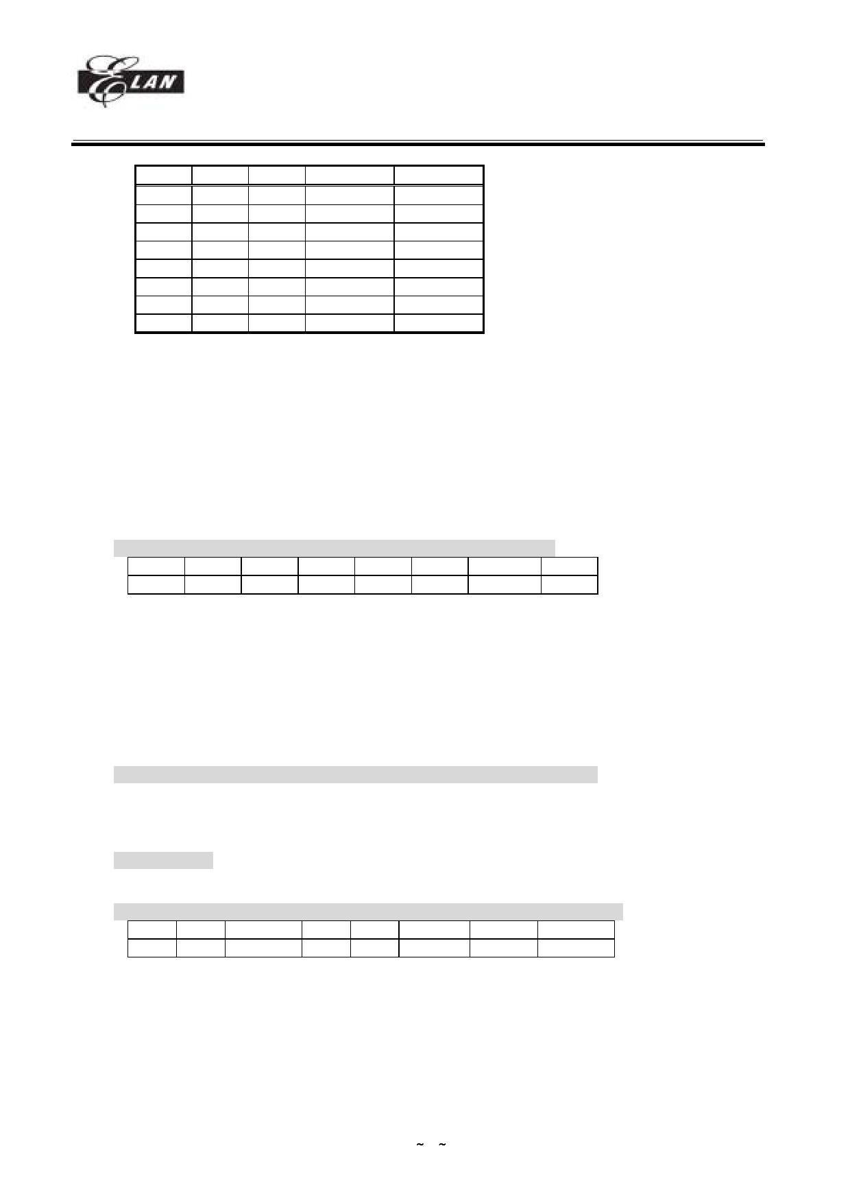
PSR2 PSR1 PSR0 TCC Rate WDT Rate
0
0
0
1:2
1:1
0
0
1
1:4
1:2
0
1
0
1:8
1:4
0
1
1
1:16
1:8
1
0
0
1:32
1:16
1
0
1
1:64
1:32
1
1
0
1:128
1:64
1
1
1
1:256
1:128
* Bit 3 (PAB) : Prescaler assignment bit, 0/1 ! prescaler for TCC/prescaler for WDT
* Bit 4 (TE) : TCC signal edge
0 ! increment from low to high transition on TCC
1 ! increment from high to low transition on TCC
* Bit 4 : unused
* Bit 5 (TS) : TCC signal source, 0/1 ! internal instruction cycle clock/16.384kHz
* Bit 6 (INT) : INT enable flag
0 ! interrupt masked by DISI or hardware interrupt
1 ! interrupt enable by ENI/RETI instructions
* Bit 7 (INT_EDGE) : Interrupt edge control of P70, 0/1 ! rising edge interrupt/falling interrupt
CONT register is readable and writable.
3. IOC5 (PORT5(7:4) I/O control, MEI and RTF output, RTF power control)
7
6
5
4
3
2
1
0
IOC57 IOC56 IOC55 IOC54 MEIO RTFO RTFPWR 0
* Bit 0 = 0 : unused
* Bit 1 (RTFPWR) : Power control of RTF circuit, 1/0 ! power on/power off
* Bit 2 (RTFO) : (Read Only) RTF line DC voltage change detect output.
When line DC voltage is not changed, RTFO is high.
* Bit3 (MEIO) : (Read Only) MEI line high or line in-use detect output
When input voltage of MEI pin is below 1.2V, MEIO is low; when input voltage of MEI pin is over 1.3V,
MEIO is high.
* Bit 4 ~7 (IOC54 ~ IOC57) : PORT5 I/O direction control registers.
“1” put the relative I/O pin into high impedance, while “0” put the relative I/O pin as output.
4. IOC6, IOC7 and IOC9 (I/O port control register for PORT6, PORT7 and PORT9)
IOC6, IOC7 and IOC9 are four I/O direction control registers for PORT6, PORT7 and PORT9.
"1" put the relative I/O pin into high impedance, while "0" put the relative I/O pin as output.
User can see IOCB register how to switch to normal I/O port.
5. IOC8 (unused)
IOC8 is unused and always “00000000”.
6. IOCA (CALLER ID RAM,IO ,PAGE Control Register)(read/write,initial "00000000")
7
6
5
4
3
2
1
0
0
0 SDTPW/0 0
0 CALL_2 CALL_1 MEIPWR
* Bit 0(MEIPWR) : power control of MEI circuit, 1/0 ! power on/power off
* Bit 2,1 (CALL_2,CALL_1) : Bank selections for Caller ID RAM
00 to 11 are four blocks of CALLER ID RAM area. User can use 1.0K RAM by RC register.
* Bit 3~4 = 0 : unused
* Bit 5 (SDTPW/0) : Power control of Stuttered dial tone circuit/disable SDT
ps. When code option bit2(/SDTEN) is “1”, SDT is disabled and IOCA bit5 is always “0”. User cannot
use SDT function. When code option bit2(/SDTEN) is “0”, SDT is enabled and IOCA bit5 is
SDTPW. At this time, setting SDTPW 1/0 ! power on SDT circuit /power down SDT circuit.
__________________________________________________________________________________________________________________________________________________________________
* This specification are subject to be changed without notice.
~ 11~
2001/01/12
Share Link: 