EM78871H Ver la hoja de datos (PDF) - ELAN Microelectronics
Número de pieza
componentes Descripción
Fabricante
EM78871H Datasheet PDF : 59 Pages
| |||
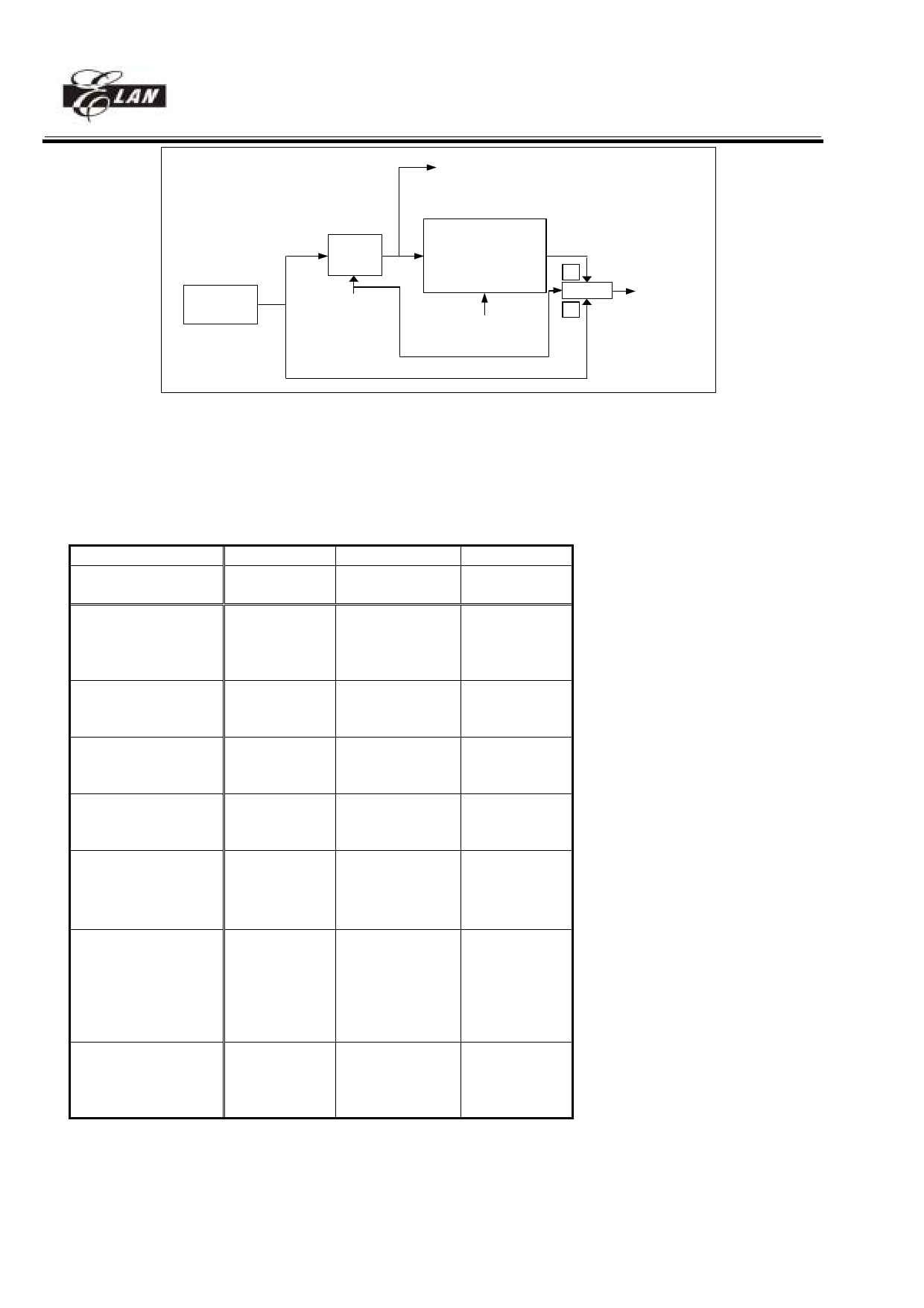
Sub-clock
32.768kHz
PLL
ENPLL
3.5826MHz to analog circuit
EM78871
8-bit Micro-controller
÷ 4 =>895.658kHz
÷ 2 =>1.7913MHz
× 1 =>3.5826MHz
× 3 =>10.7479MHz
CLK1 ~ CLK0
1
switch
0
System clock
Fig.10 The relation between 32.768kHz and PLL
Bit 7(SLEEP_N) : Power saving mode control register
When PLL is disabled, user can set this bit after using "SLEP" instruction for SLEEP mode or IDLE mode selection
0 SLEEP mode
1 Don’t allowed this setting
This bit will decide SLEP instruction which mode to go.
The status after wake-up and the wake-up sources list as the table below.
Wakeup signal
SLEEP mode GREEN mode NORMAL mode
RA(7,6)=(0,0) RA(7,6)=(x,0) RA(7,6)=(x,1)
+ SLEP
no SLEP
no SLEP
TCC time out
No function Interrupt
Interrupt
IOCF bit 0=1
(jump to address 8 (jump to address
And "ENI"
at page0)
8 at page0)
COUNTER1 time out No function
IOCF bit 1=1
And "ENI"
Interrupt
Interrupt
(jump to address 8 (jump to address
at page0)
8 at page0)
COUNTER2 time out No function
IOCF bit 2=1
And "ENI"
Interrupt
Interrupt
(jump to address 8 (jump to address
at page0)
8 at page0)
WDT time out
PORT7
IOCF bit3 or bit4 or
bit5 = 1
And "ENI"
RESET and RESET and Jump RESET and
Jump to address to address 0
Jump to address
0
0
RESET and Interrupt
Interrupt
Jump to address (jump to address 8 (jump to address
0
at page0)
8 at page0)
IOCE page2 bit 6 = 1
And RE page1 bit6
logic level variation
(switch by EDGE bit)
And “ENI”
Stack overflow
IOC5 page2 bit7=1
&bit 6: 0 1
And “ENI”
No function
No function
Interrupt
Interrupt
(jump to address 8 (jump to address
at page0)
8 at page0)
Interrupt
Interrupt
(jump to address 8 (jump to address
at page0)
8 at page0)
<Note> Stack overflow interrupt function is exist in ROM less and OTP chip only.
<Note> PORT70 ~ PORT73 's wakeup function is controlled by IOCF bit3 and ENI instruction. They are falling edge
trigger.
PORT74 ~ PORT76 's wakeup function is controlled by IOCF bit4 and ENI instruction. They are falling edge trigger.
__________________________________________________________________________________________________________________________________________________________________
* This specification is subject to be changed without notice. 20
8/23/04 (V1.5)
Share Link: 