EL2021 Ver la hoja de datos (PDF) - Intersil
Número de pieza
componentes Descripción
Fabricante
EL2021 Datasheet PDF : 8 Pages
| |||
EL2021
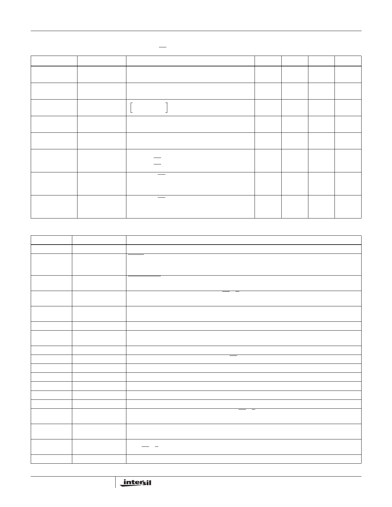
AC Electrical Specifications DC test conditions apply except where noted. For AC tests, RL = 1k, CL = 200pF. Delay times are
measured from OE or Data crossing 2.5V, VCH = 5V, VCL = 0.
PARAMETER
DESCRIPTION
CONDITIONS
MIN
TYP
MAX
UNITS
SR+
+Slew Rate
Data L to H, Output from 0.5V to 4.5V, VSR = 1V
VSR = 3V
80
100
120
V/µs
150
240
360
V/µs
SR-
SRSYM
-Slew Rate
Slew Rate
Symmetry
Data H to L, Output from 4.5V to 0.5V, VSR = 1V
VSR = 3V
-(---S----R-----+----)------(--S-----R--------)- VSR = 1V
(SR+)+(SR-) VSR = 2V
-80
-150
-10
-20
-100
-240
-120
-360
10
20
V/µs
V/µs
%
%
TPD
Propagation Delay Data L to H, Output to 0.2V, VSR = 2.5V
Data H to L, Output to 4.8V, VSR = 2.5V
6.5
9
11.5
ns
6.5
9
11.5
ns
TS
Settling Time
VSR = 5V, Data L to H, Output 4.5V to 5V±0.2V
VSR = 5V, Data H to L, Output 0.5V to ±0.2V
30
ns
30
ns
OS
TPDA
TPDH
Overshoot
VSR = 1V, Data L to H or H to L
VSR = 1V, OE H to L, Data = L, RL to 5V
VSR = 1V, OE H to L, Data = H, RL to 0V
Propagation Delay, VSR = 2.5V, OE H to L, CL = 50pF
High-Z to Active RL to 5V, Data = L, Output to 3.5V
RL to 0V, Data = H, Output to 1.5V
Propagation Delay, VSR = 2.5V, OE L to H, CL = 50pF,
Active to High-Z Data = L, RL to 5V, Output to 0.5V
Data = H, RL to 0V, Output to 4.5V
-300
-300
-300
300
mV
300
mV
300
mV
50
ns
50
ns
50
ns
50
ns
Pin Description Table
PIN #
NAME
1
GND
2
E
3
OE
4
VCL
5
B-
6
ISENSE-
7
V-
8
Drive-
9
VOUT
10
Drive+
11
Sense Out
12
V+
13
ISENSE+
14
B+
15
VCH
16
VSR
17
Data
18
N/C
DESCRIPTION
System ground.
Enable control input. A logic low allows normal operation; a logic high puts the device into
power down mode. No output levels are defined in powerdown nor does the output behave
as a high impedance.
Output Enable input. A logic low sets the output to low-impedance driver mode; a logic high
places the output into a high-impedance state.
Lower analog control input. When Data = OE = E = L, the VCL level is output as VOUT
(assuming VCL < VCH).
System power supply. The EL2021 uses this pin as a negative output current monitor connection.
Little current is drawn from this pin, transient or static.
Negative output current monitor input.
Negative power supply. Because all negative output drive currents come from this pin
(as much as 60mA transiently), good bypassing is essential.
Output to external pnp transistor base.
High-current input and output, depending on OE.
Output to external npn transistor base.
Logic output which signals that a high + or - output current is flowing.
Positive power supply. Like V-, it should be well bypassed.
Positive output current monitor input.
System power supply, similar to B-.
Higher analog control input. When Data = H and OE = E = L, the VCH level is output as
VOUT (assuming VCH > VCL).
Slew rate control input. A 1V level on this pin causes the output to slew at 100V/µs, 0.5V
causes a slew rate of 50V/µs, etc.
Output level control input. This pin digitally selects VCL or VCH as the output voltage
when OE = E = L.
Not Connected.
3
Share Link: 