29F0408 Ver la hoja de datos (PDF) - MAXWELL TECHNOLOGIES
Número de pieza
componentes Descripción
Fabricante
29F0408 Datasheet PDF : 32 Pages
| |||
32 Megabit (4M x 8-Bit) Flash Memory
29F0408
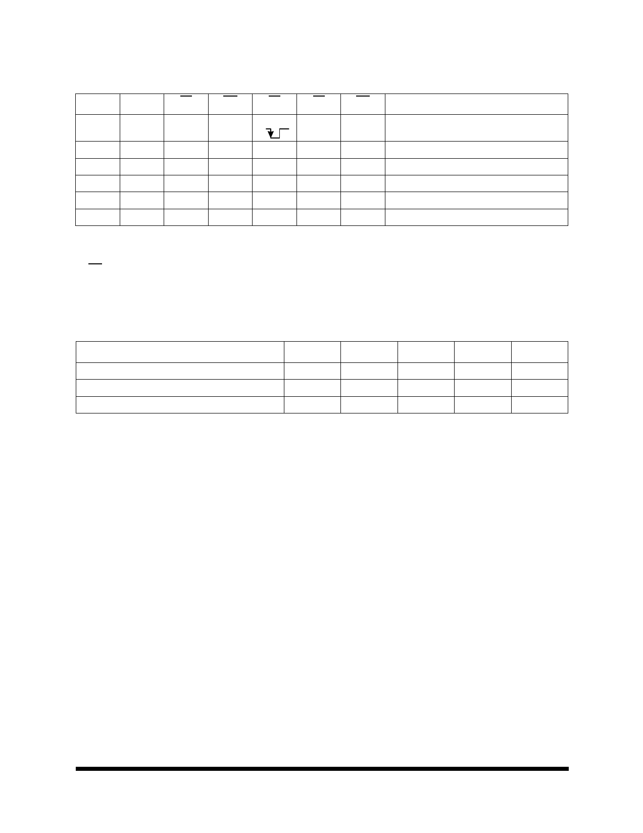
TABLE 8. 29F0408 MODE SELECTION
CLE
ALE
CE
WE
RE
SE
WP
MODE
L
L
L
H
L/H 1
X Sequential Read & Data Output
L
L
L
H
H
L/H 1
X
X
X
X
X
L/H 1
X
X
X
X
X
X
X
X2
X
X
X
X
X
X
H
X
X
0V/VCC3
1. When SE is high, spare area is deselected.
2. X can be VIL or VIH.
3. WP should be biased to CMOS high or CMOS low for standby.
X During Read (Busy)
H During Program (Busy)
H During Erase (Busy)
L Write Protect
0V/VCC3 Stand-by
TABLE 9. 29F0408 PROGRAM/ERASE CHARACTERISTICS
(VCC = 5 V ± 10%, TA =-40 TO +125C, UNLESS OTHERWISE NOTED)
PARAMETER
SYMBOL
MIN
TYP
MAX
Program time
tPROG
--
0.25
1.5
Number of partial program cycles in the same page
NOP
--
--
10
Block erase time
tBERS
--
2
10
UNIT
ms
cycles
ms
11.08.02 Rev 2
All data sheets are subject to change without notice 5
©2002 Maxwell Technologies
All rights reserved.
Share Link: 