CXA3067 Ver la hoja de datos (PDF) - Sony Semiconductor
Número de pieza
componentes Descripción
Fabricante
CXA3067 Datasheet PDF : 24 Pages
| |||
CXA3067M
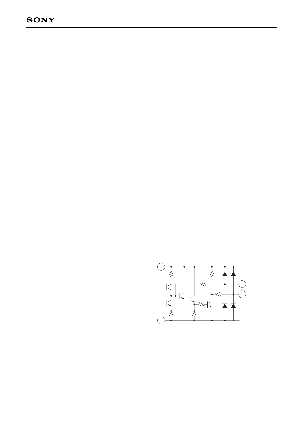
Notes on Application
Take care of the followings because the CXA3067M has limiter voltage gain of approximately 67 dB and uses
high frequency.
1) Separate the input pattern from the output pattern as far as possible and makes wiring short.
2) Ground the decoupling capacitor as close to pin 13 as possible.
Take care of the followings in order to reduce the jitter.
1) Insert the capacitor as close to pin 17 and 18 as possible.
2) Ground the by-pass capacitor as close to IFVCC to supply pin 16 as possible.
Take care of the following, for the purpose of the isolation of local oscillator resonance circuit and X’tal (RFF
CLOCK).
1) Separate the patterns connected pin 1 and pin 2 from the local oscillator resonance circuit.
Take care of the following, in order to reduce the phase noise.
1) Connect the loop filter as close to pins 5 and 6 as possible.
Take care of the following, in order to prevent the parasitic oscillation.
1) Connect the local oscillator resonance circuit as close to pins 7 and 8 as possible.
And compact the local oscillator resonance circuit.
The tuning voltage at the local oscillator resonance circuit.
The output voltage at pin 6 is 0.3 V to VCC.
When the oscillation frequency is the desired frequency, please the output voltage at pin 6 should be been 2.5 V.
Please decide the component value of loop filter by each system.
DVCC
11
10k
100
5
100
6
9
DGND
—17—
Share Link: 