TSA5526AM/C2 Ver la hoja de datos (PDF) - Philips Electronics
Número de pieza
componentes Descripción
Fabricante
TSA5526AM/C2 Datasheet PDF : 28 Pages
| |||
Philips Semiconductors
1.3 GHz universal bus-controlled
TV synthesizers
Product specification
TSA5526; TSA5527
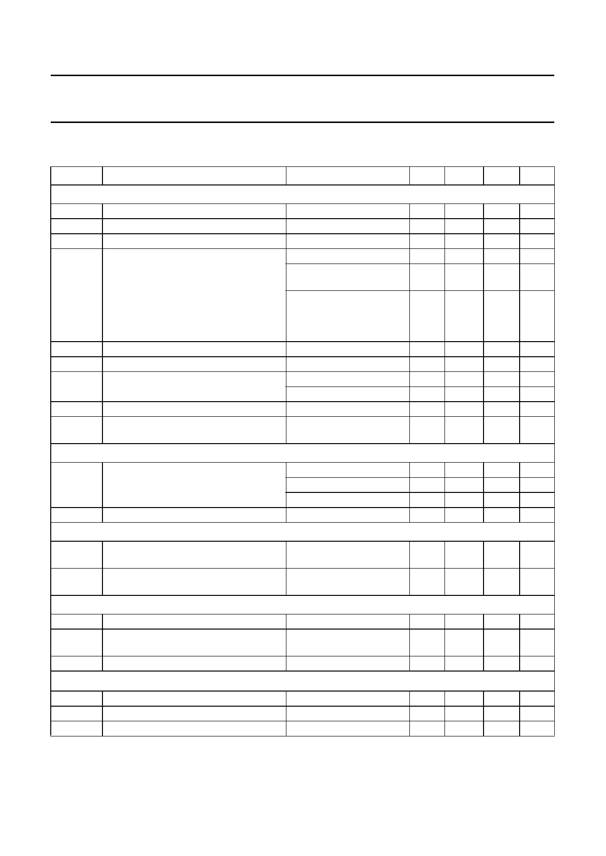
CHARACTERISTICS
VCC1 = 4.5 to 5.5 V; VCC2 = VCC1 to 13.2 V; Tamb = −20 to +85 °C; unless otherwise specified.
SYMBOL
PARAMETER
CONDITIONS
MIN. TYP. MAX. UNIT
Supplies
VCC1
VCC2
ICC1
ICC2
VPOR
fRF
DR
fxtal
Zxtal
supply voltage
4.5
band switch buffers supply voltage
supply current
at power-on
VCC1
−
band switch buffers supply current
at power-on
−
one band switch buffer is −
ON; Isource = 40 mA
two band switch buffers are −
ON;
Isource = 40 mA + 5 mA
(any combination)
supply voltage below which POR is active
1.5
RF input frequency
64
divider ratio
15-bit frequency word
256
14-bit frequency word
256
crystal oscillator input frequency
Rxtal = 25 to 300 Ω
3.2
crystal oscillator input impedance
fi = 4 MHz
600
(absolute value)
−
−
20
0.5
50
56
2.0
−
−
−
4
1 200
5.5 V
13.5 V
25
mA
1.0 mA
55
mA
62
mA
−
V
1300 MHz
32 767
1 6 383
4.48 MHz
−
Ω
Prescaler (see Figs 6 and 7)
Vi(RF)
RF input level
Zi(RF)
input impedance
fi = 80 to 150 MHz
fi = 150 to 1000 MHz
fi = 1000 to 1300 MHz
see Fig.8
−25 −
−28 −
−15 −
3
dBm
3
dBm
3
dBm
PNP band switch buffers outputs (pins 5 to 8)
ILO
Vo(sat)
output leakage current
output saturation voltage
VCC2 = 13.5 V;
Vo = 0 V
Isource = 40 mA;
Vo(sat) = VCC2 − Vo
−10 −
−
0.2
−
µA
0.4 V
LOCK output (PNP collector output) 3 wire bus mode (pin 12)
Io(ool)
Vosat(ool)
Vo(LOCK)
output current when out-of-lock
output saturation voltage when
out-of-lock
lock output voltage
VCC1 = 5.5 V; Vo = 5.5 V −
Isource = 200 µA;
−
Vo(sat) = VCC1 − Vo
−
−
100 µA
0.4
0.8 V
0.01 0.4 V
ADC input (I2C-bus mode) pin 12
Vi(ADC)
IIH(ADC)
IIL(ADC)
ADC input voltage
HIGH level input current
LOW level input current
see Table 9
VADC = VCC1
VADC = 0 V
0
−
−
−
−10 −
VCC1 V
10
µA
−
µA
1996 Sep 24
12
Share Link: 