CM1293 Ver la hoja de datos (PDF) - ON Semiconductor
Número de pieza
componentes Descripción
Fabricante
CM1293 Datasheet PDF : 7 Pages
| |||
CM1293
8-Channel Low
Capacitance ESD
Protection Arrays
Product Description
The CM1293 family of diode arrays has been designed to provide
ESD protection for electronic components or sub−systems requiring
minimal capacitive loading. These devices are ideal for protecting
systems with high data and clock rates or for circuits requiring low
capacitive loading. Each ESD channel consists of a pair of diodes in
series which steer the positive or negative ESD current pulse to either
the positive (VP) or negative (VN) supply rail. A Zener diode is
embedded between VP and VN, offering two advantages. First, it
protects the VCC rail against ESD strikes, and second, it eliminates the
need for a bypass capacitor that would otherwise be needed for
absorbing positive ESD strikes to ground. The CM1293 will protect
against ESD pulses up to (8 kV contact discharge) per the
IEC 61000−4−2 Level 4 standard.
This device is particularly well−suited for protecting systems using
high−speed ports such as USB2.0, IEEE1394 (FireWire®, i.LINKt),
Serial ATA, DVI, HDMI and corresponding ports in removable
storage, digital camcorders, DVD−RW drives and other applications
where extremely low loading capacitance with ESD protection are
required in a small package footprint.
Features
• Eight Channels of ESD Protection
Note: For 2 and 4 Channel Devices, See the CM1293A Datasheet
• Provides ESD Protection to IEC61000−4−2
• ±8 kV Contact Discharge
• Low Loading Capacitance of 2.0 pF Max
• Low Clamping Voltage
• Channel I/O to I/O Capacitance 1.5 pF Typical
• Zener Diode Protects Supply Rail and Eliminates the Need for
External By−Pass Capacitors
• Each I/O Pin Can Withstand over 1000 ESD Strikes*
• These Devices are Pb−Free and are RoHS Compliant
Applications
• DVI Ports, HDMI Ports in Notebooks, Set Top Boxes, Digital TVs,
LCD Displays
• Serial ATA Ports in Desktop PCs and Hard Disk Drives
• PCI Express Ports
• General Purpose High−Speed Data Line ESD Protection
http://onsemi.com
MSOP−10
MR SUFFIX
CASE 846AE
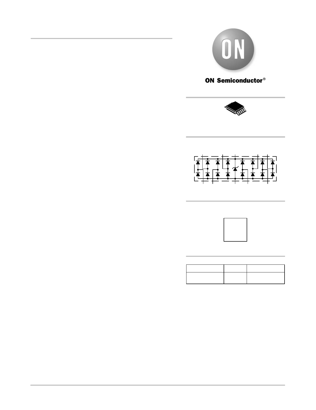
BLOCK DIAGRAM
CH8
CH7 VP
CH6 CH5
CH1 CH2
VN CH3
CM1293−08MR
CH4
MARKING DIAGRAM
D039
D039 = CM1293−08MR
ORDERING INFORMATION
Device
Package
Shipping†
CM1293−08MR MSOP−10 4000/Tape & Reel
(Pb−Free)
†For information on tape and reel specifications,
including part orientation and tape sizes, please
refer to our Tape and Reel Packaging Specification
Brochure, BRD8011/D.
*Standard test condition is IEC61000−4−2 level 4 test circuit with each pin subjected to ±8 kV contact discharge for 1000 pulses. Discharges
are timed at 1 second intervals and all 1000 strikes are completed in one continuous test run. The part is then subjected to standard production
test to verify that all of the tested parameters are within spec after the 1000 strikes.
© Semiconductor Components Industries, LLC, 2011
1
March, 2011 − Rev. 4
Publication Order Number:
CM1293/D
Share Link: 