APM4532(2003) Ver la hoja de datos (PDF) - Anpec Electronics
Número de pieza
componentes Descripción
Fabricante
APM4532 Datasheet PDF : 13 Pages
| |||
APM4532
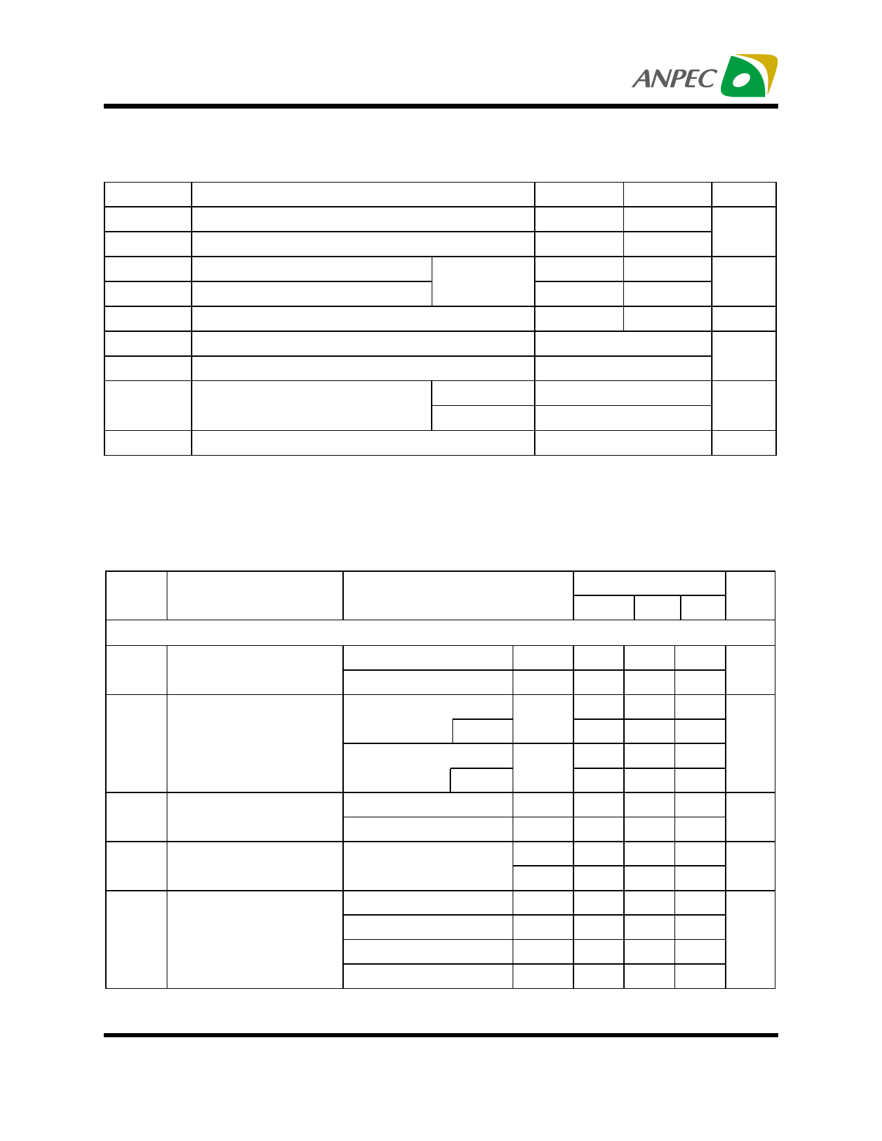
Absolute Maximum Ratings (TA = 25°C unless otherwise noted)
Symbol
Parameter
VDSS
VGSS
ID*
IDM
Drain-Source Voltage
Gate-Source Voltage
Maximum Drain Current – Continuous
Maximum Drain Current – Pulsed
PD Maximum Power Dissipation
TA=25°C
TA=100°C
TJ Maximum Junction Temperature
TSTG
RθjA
Storage Temperature Range
Thermal Resistance – Junction to Ambient
* Surface Mounted on FR4 Board, t ≤ 10 sec.
N-Channel P-Channel
30
-30
±25
±25
5
-3.5
20
-20
2
2
0.8
0.8
150
-55 to 150
62.5
Unit
V
A
W
°C
°C
°C/W
Electrical Characteristics (TA = 25°C unless otherwise noted)
Symbol
Parameter
Test Condition
Static
BVDSS
Drain-Source Breakdown
Voltage
IDSS
Zero Gate Voltage Drain
Current
VGS(th) Gate Threshold Voltage
VGS=0V , IDS=250µA
VDS=24V , VGS=0V
VDS=-24V , VGS=0V
VDS=VGS , IDS=250µA
VDS=VGS , IDS=-250µA
IGSS Gate Leakage Current
VGS=±25V , VDS=0V
RDS(ON)a
Drain-Source On-state
Resistance
VSDa Diode Forward Voltage
VGS=10V , IDS=5A
VGS=4.5V , IDS=4A
VGS=-10V , IDS=-3.5A
VGS=-4.5V , IDS=-2.5A
ISD=1.7A , VGS=0V
ISD=-1.7A , VGS=0V
Notes
a : Pulse test ; pulse width ≤300µs, duty cycle ≤ 2%
APM4532
Unit
Min. Typ. Max.
N-Ch 30
P-Ch -30
N-Ch
P-Ch
V
1
µA
-1
N-Ch 1 1.5 2
V
P-Ch -1 -1.5 -2
N-Ch
P-Ch
±100 nA
±100
N-Ch
P-Ch
35 45
60 70
mΩ
85 95
135 150
N-Ch
P-Ch
0.7 1.3 V
-0.7 -1.3
Copyright ANPEC Electronics Corp.
2
Rev. A.1 - Sep., 2002
www.anpec.com.tw
Share Link: 