ATMEGA329/V_06 Ver la hoja de datos (PDF) - Atmel Corporation
Número de pieza
componentes Descripción
Fabricante
ATMEGA329/V_06 Datasheet PDF : 28 Pages
| |||
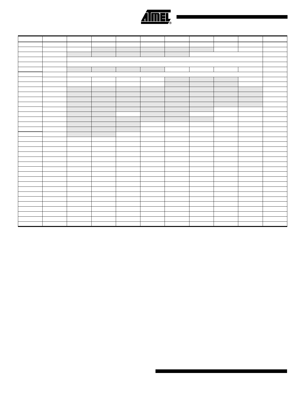
Address
0x24 (0x44)
0x23 (0x43)
0x22 (0x42)
0x21 (0x41)
0x20 (0x40)
0x1F (0x3F)
0x1E (0x3E)
0x1D (0x3D)
0x1C (0x3C)
0x1B (0x3B)
0x1A (0x3A)
0x19 (0x39)
0x18 (0x38)
0x17 (0x37)
0x16 (0x36)
0x15 (0x35)
0x14 (0x34)
0x13 (0x33)
0x12 (0x32)
0x11 (0x31)
0x10 (0x30)
0x0F (0x2F)
0x0E (0x2E)
0x0D (0x2D)
0x0C (0x2C)
0x0B (0x2B)
0x0A (0x2A)
0x09 (0x29)
0x08 (0x28)
0x07 (0x27)
0x06 (0x26)
0x05 (0x25)
0x04 (0x24)
0x03 (0x23)
0x02 (0x22)
0x01 (0x21)
0x00 (0x20)
Name
TCCR0A
GTCCR
EEARH
EEARL
EEDR
EECR
GPIOR0
EIMSK
EIFR
Reserved
Reserved
Reserved
Reserved
TIFR2
TIFR1
TIFR0
PORTG
DDRG
PING
PORTF
DDRF
PINF
PORTE
DDRE
PINE
PORTD
DDRD
PIND
PORTC
DDRC
PINC
PORTB
DDRB
PINB
PORTA
DDRA
PINA
Bit 7
FOC0A
TSM
-
-
PCIE3
PCIF3
-
-
-
-
-
-
-
-
-
-
PORTF7
DDF7
PINF7
PORTE7
DDE7
PINE7
PORTD7
DDD7
PIND7
PORTC7
DDC7
PINC7
PORTB7
DDB7
PINB7
PORTA7
DDA7
PINA7
Bit 6
WGM00
-
-
-
PCIE2
PCIF2
-
-
-
-
-
-
-
-
-
-
PORTF6
DDF6
PINF6
PORTE6
DDE6
PINE6
PORTD6
DDD6
PIND6
PORTC6
DDC6
PINC6
PORTB6
DDB6
PINB6
PORTA6
DDA6
PINA6
Bit 5
COM0A1
-
-
-
PCIE1
PCIF1
-
-
-
-
-
ICF1
-
-
-
PING5
PORTF5
DDF5
PINF5
PORTE5
DDE5
PINE5
PORTD5
DDD5
PIND5
PORTC5
DDC5
PINC5
PORTB5
DDB5
PINB5
PORTA5
DDA5
PINA5
Bit 4
Bit 3
COM0A0
WGM01
-
-
-
-
EEPROM Address Register Low
EEPROM Data Register
-
EERIE
General Purpose I/O Register
PCIE0
-
PCIF0
-
-
-
-
-
-
-
-
-
-
-
-
-
-
-
PORTG4
PORTG3
DDG4
DDG3
PING4
PING3
PORTF4
PORTF3
DDF4
DDF3
PINF4
PINF3
PORTE4
PORTE3
DDE4
DDE3
PINE4
PINE3
PORTD4
PORTD3
DDD4
DDD3
PIND4
PIND3
PORTC4
PORTC3
DDC4
DDC3
PINC4
PINC3
PORTB4
PORTB3
DDB4
DDB3
PINB4
PINB3
PORTA4
PORTA3
DDA4
DDA3
PINA4
PINA3
Bit 2
Bit 1
Bit 0
CS02
CS01
CS00
-
PSR2
PSR10
EEPROM Address Register High
EEMWE
-
-
-
-
-
-
-
OCF1B
-
PORTG2
DDG2
PING2
PORTF2
DDF2
PINF2
PORTE2
DDE2
PINE2
PORTD2
DDD2
PIND2
PORTC2
DDC2
PINC2
PORTB2
DDB2
PINB2
PORTA2
DDA2
PINA2
EEWE
-
-
-
-
-
-
OCF2A
OCF1A
OCF0A
PORTG1
DDG1
PING1
PORTF1
DDF1
PINF1
PORTE1
DDE1
PINE1
PORTD1
DDD1
PIND1
PORTC1
DDC1
PINC1
PORTB1
DDB1
PINB1
PORTA1
DDA1
PINA1
EERE
INT0
INTF0
-
-
-
-
TOV2
TOV1
TOV0
PORTG0
DDG0
PING0
PORTF0
DDF0
PINF0
PORTE0
DDE0
PINE0
PORTD0
DDD0
PIND0
PORTC0
DDC0
PINC0
PORTB0
DDB0
PINB0
PORTA0
DDA0
PINA0
Page
99
104/151
20
20
20
20
24
56
57
149
131
102
88
88
88
87
87
87
87
87
87
87
87
87
86
86
86
86
86
86
86
86
86
Note:
1. For compatibility with future devices, reserved bits should be written to zero if accessed. Reserved I/O memory addresses
should never be written.
2. I/O Registers within the address range 0x00 - 0x1F are directly bit-accessible using the SBI and CBI instructions. In these
registers, the value of single bits can be checked by using the SBIS and SBIC instructions.
3. Some of the Status Flags are cleared by writing a logical one to them. Note that, unlike most other AVRs, the CBI and SBI
instructions will only operate on the specified bit, and can therefore be used on registers containing such Status Flags. The
CBI and SBI instructions work with registers 0x00 to 0x1F only.
4. When using the I/O specific commands IN and OUT, the I/O addresses 0x00 - 0x3F must be used. When addressing I/O
Registers as data space using LD and ST instructions, 0x20 must be added to these addresses. The
ATmega329/3290/649/6490 is a complex microcontroller with more peripheral units than can be supported within the 64
location reserved in Opcode for the IN and OUT instructions. For the Extended I/O space from 0x60 - 0xFF in SRAM, only
the ST/STS/STD and LD/LDS/LDD instructions can be used.
12 ATmega329/3290/649/6490
2552HS–AVR–11/06
Share Link: 