ATA6622-PGPW(2008) Ver la hoja de datos (PDF) - Atmel Corporation
Número de pieza
componentes Descripción
Fabricante
ATA6622-PGPW Datasheet PDF : 29 Pages
| |||
ATA6622/ATA6624/ATA6626
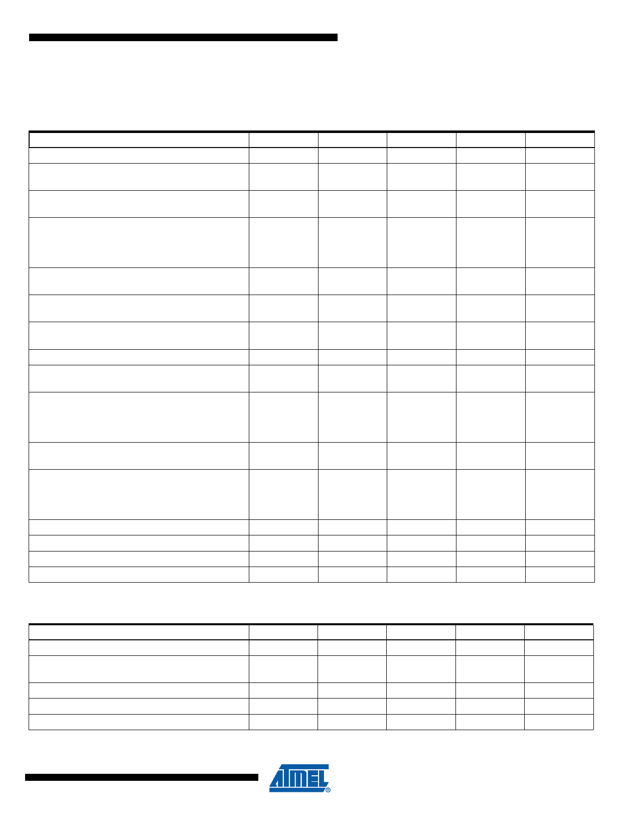
7. Absolute Maximum Ratings
Stresses beyond those listed under “Absolute Maximum Ratings” may cause permanent damage to the device. This is a stress rating
only and functional operation of the device at these or any other conditions beyond those indicated in the operational sections of this
specification is not implied. Exposure to absolute maximum rating conditions for extended periods may affect device reliability.
Parameters
Symbol
Min.
Typ.
Max.
Unit
Supply voltage VS
Pulse time ≤ 500 ms
Ta = 25°C
Output current IVCC ≤ 50 mA
Pulse time ≤ 2 min
Ta = 25°C
Output current IVCC ≤ 50 mA
WAKE (with 33 kΩ serial resistor)
KL_15 (with 50 kΩ/100 nF)
DC voltage
Transient voltage due to ISO7637
(coupling 1 nF)
VS
–0.3
VS
VS
–1
–150
+40
V
+40
V
27
V
+40
V
+100
V
INH
- DC voltage
–0.3
+40
V
LIN
- DC voltage
–27
+40
V
Logic pins (RxD, TxD, EN, NRES, NTRIG,
WD_OSC, MODE, TM)
–0.3
+5.5
V
Output current NRES
PVCC DC voltage
VCC DC voltage
INRES
–0.3
–0.3
+2
mA
+5.5
V
+6.5
V
According to IBEE LIN EMC
Test Spec. 1.0 following IEC 61000-4-2
- Pin VS, LIN to GND
±6
KV
- Pin WAKE (33 kΩ serial resistor) to GND
±5
KV
HBM ESD
ANSI/ESD-STM5.1
JESD22-A114
±3
KV
AEC-Q100 (002)
CDM ESD STM 5.3.1
±750
V
ESD HBM following STM5.1 with 1.5 kΩ
150 pF
±8
KV
- Pin VS, LIN, WAKE to GND
Junction temperature
Tj
–40
Storage temperature
Ts
–55
Thermal resistance junction to heat slug
Rthjc
Thermal resistance junction to ambient,
where heat slug is soldered to PCB
Rthja
+150
°C
+150
°C
10
K/W
35
K/W
Thermal shutdown of VCC regulator
150
165
170
°C
Thermal shutdown of LIN output
150
165
170
°C
Thermal shutdown hysteresis
10
°C
17
4986F–AUTO–07/08
Share Link: 