AS1310-BTDT-XX2 Ver la hoja de datos (PDF) - austriamicrosystems AG
Número de pieza
componentes Descripción
Fabricante
AS1310-BTDT-XX2
austriamicrosystems AG

AS1310-BTDT-XX2 Datasheet PDF : 20 Pages
| |||
AS1310
Datasheet - Application Information
9 Application Information
The AS1310 is available with fixed output voltages from 1.8V to 3.3V in 50mV steps.
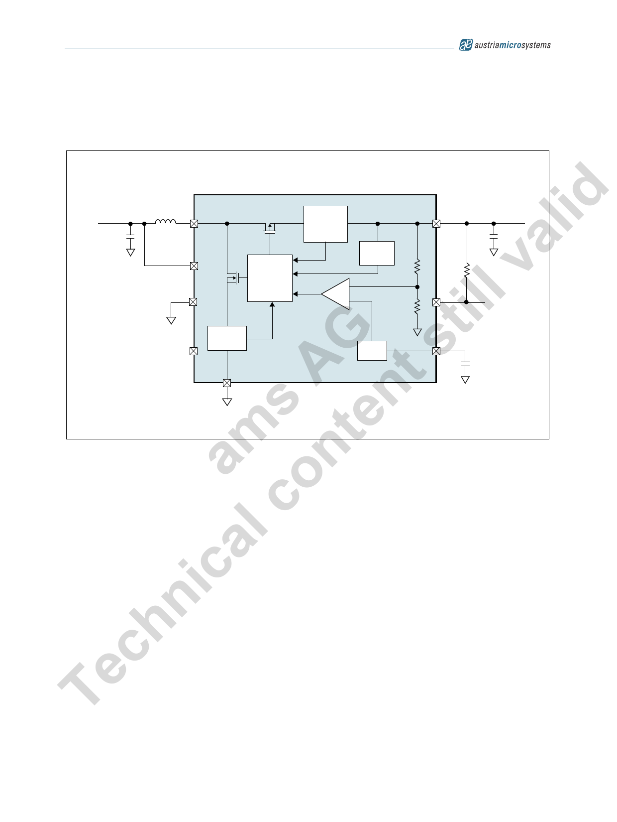
Figure 14. AS1310 Block Diagram
lid 0.7 to 3.6V
Input
CIN
AG t still va 22µF
6.8µH
LX
VIN
LBI
EN
Driver
and
Control
Logic
Zero
Crossing
Detector
Startup
Circuitry
–
+
Imax
Detection
AS1310
VREF
GND
VOUT
1.8V to 3.3V
Output
COUT
22µF
R3
LBO
REF
CREF
100nF
ms ten 9.1 AS1310 Features
a n Shutdown. The part is in shutdown mode while the voltage at pin EN is below 0.1V and is active when the voltage is higher than 0.7V.
o Note: EN can be driven above VIN or VOUT, as long as it is limited to less than 3.6V.
c Output Disconnect and Inrush Limiting. During shutdown VOUT is going to 0V and no current from the input source is running through
the device. This is true as long as the input voltage is higher than the output voltage.
l Feedthrough Mode. If the input voltage is higher than the output voltage the supply voltage is connected to the load through the device. To
a guarantee a proper function of the AS1310 it is not allowed that the supply exceeds the maximum allowed input voltage (3.6V).
ic In this feedthrough mode the quiescent current is 35µA (typ.). The device goes back into step-up mode when the oputput voltage is 4% (typ.)
Techn below VOUTNOM.
www.austriamicrosystems.com/DC-DC_Step-Up/AS1310
Revision 1.8
12 - 19
Share Link: