ARA2004S12P1 Ver la hoja de datos (PDF) - ANADIGICS
Número de pieza
componentes Descripción
Fabricante
ARA2004S12P1 Datasheet PDF : 20 Pages
| |||
ARA2004
LOGIC PROGRAMMING
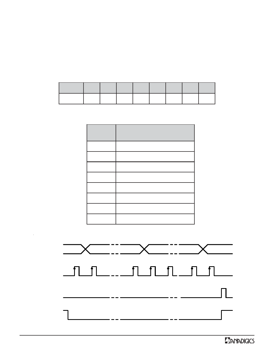
Programming Instructions
The programming word is set through an 8 bit shift
register via the data, clock and enable lines. The
data is entered in order with the most significant bit
(MSB) first and the least significant bit (LSB) last.
The enable line must be low for the duration of the
data entry, then set high to latch the shift register.
The rising edge of the clock pulse shifts each data
value into the register.
Table 6: Programming Word
DATA BIT D7
D6
D5
D4
D3
D2
D1
D0
Value
P7 P6 P5 P4 P3 P2 P1 P0
Table 7: Data Description
VALUE
FUNCTION
(1 = on, 0 = bypass)
P7
N/A
P6
N/A
P5
32 dB Attenuator Bit
P4
16 dB Attenuator Bit
P3
8 dB Attenuator Bit
P2
4 dB Attenuator Bit
P1
2 dB Attenuator Bit
P0
1 dB Attenuator Bit
DATA
D7: MSB
D6
CLOCK
D4
D3
D1
D0: LSB
ENABLE
OR
ENABLE
12
Figure 17: Serial Data Input Timing
Data Sheet - Rev 2.1
07/2005
Share Link: 