APW7062B Ver la hoja de datos (PDF) - Anpec Electronics
Número de pieza
componentes Descripción
Fabricante
APW7062B Datasheet PDF : 18 Pages
| |||
APW7062B
Functional Pin Description
RT (Pin1)
This pin can adjust the switching frequency. Connect
a resistor from RT to GND for increasing the switching
frequency:
FS
=
200kHz
+
4.15 ×10⁶
RT
(RT to GND,FS = 200kHz to 400kHz)
Conversely, connect a resistor from RT to VCC for de-
creasing the switching frequency:
FS
=
200kHz
-
3.51 × 10 7
RT
(RT to VCC,FS = 200kHz to 75kHz)
OCSET (Pin2)
This pin serves two functions: a shutdown control and
the setting of over current limit threshold. Pulling this
pin below 1.27V will shutdown the controller, forcing
the UGATE and LGATE signals to be at 0V.
A resistor (Rocset) connected between this pin and the
drain of the high side MOSFET will determine the over
current limit. An internal 200uA current source will
flow through this resistor, creating a voltage drop,
which will be compared with the voltage across the
high side MOSFET. The threshold of the over current
limit is therefore given by:
( ) IPEAK = IOCSET 200uA R × OCSET
RDS(ON)
To avoid noise interference from switching transient, a
delay time is designed in the OCP comparator.
The over current protection is active only when the
high side MOSFET is turned on longer than 300ns.
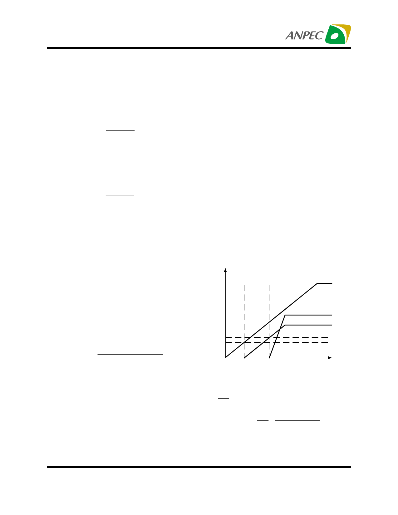
SS (Pin3)
Connect a capacitor from the pin to GND to set the
soft-start interval of the converter. An internal 10uA
current source charges this capacitor to 5.8V. The
SS voltage clamps the error amplifier output, and Fig-
ure1 shows the soft-start interval. At t1, the SS volt-
age reaches the valley of the oscillator’s triangle wave.
The PWM comparator starts to generate a PWM sig-
nal to control logic, and the output is rising rapidly.
Until the output is in regulation at t2, the clamp on the
COMP is released. This method provides a rapid and
controlled output voltage rise.
When over current protection occurs, the VOUT is
shutdown, and re-soft-start again, if the over current
condition still exists in soft-start , the VOUT is
shutdowned again, after the SS reaches 4.5V, the SS
is discharged to zero. The soft-start is recurring until
the over current condition is eliminated.
VO L TAGE
VSOFT STAR T
VOSC (M IN)
VSS= 1 .2 V
VO U T
Erro r Am p
Ou tput
t0
t1
t2
t3
TIME
FIGURE1. SOFT-START INTERVAL
I t2
=
CSS
SS
× (VOSC(MIN)+
t1)
= − = × × tSoftStart t3 t2
CSS V OUT SteadyState ∆VOSC
ISS
VIN
Copyright ANPEC Electronics Corp.
5
Rev. A.3 - Mar., 2005
www.anpec.com.tw
Share Link: 