APL5910 Ver la hoja de datos (PDF) - Anpec Electronics
Número de pieza
componentes Descripción
Fabricante
APL5910 Datasheet PDF : 17 Pages
| |||
APL5910
Layout Consideration (See figure 1)
1. Please solder the Exposed Pad on the system ground
pad on the top-layer of PCBs. The ground pad must
have wide size to conduct heat into the ambient air
through the system ground plane and PCB as a heat
sink.
2. Please place the input capacitors for VIN and VCNTL
pins near the pins as close as possible for decoupling
high-frequency ripples.
3. Ceramic decoupling capacitors for load must be
placed near the load as close as possible for
decoupling high-frequency ripples.
4. To place APL5910 and output capacitors near the load
reduces parasitic resistance and inductance for ex-
cellent load transient reponse.
5. The negative pins of the input and output capacitors
and the GND pin must be connected to the ground
plane of the load.
6. Large current paths, shown by bold lines on the fig-
ure 1, must have wide tracks.
7. Place the R1, R2, and C1 near the APL5910 as close
as possible to avoid noise coupling.
8. Connect the ground of the R2 to the GND pin by using
a dedicated track.
9. Connect the one pin of the R1 to the load for Kelvin
sensing.
10. Connect one pin of the C1 to the VOUT pin for reliable
feedback compensation.
CCNTL
VCNTL
VCNTL
VIN
APL5910
VOUT
GND
C1
(Optional)
FB
R2
CIN
COUT
R1
VIN
VOUT
Load
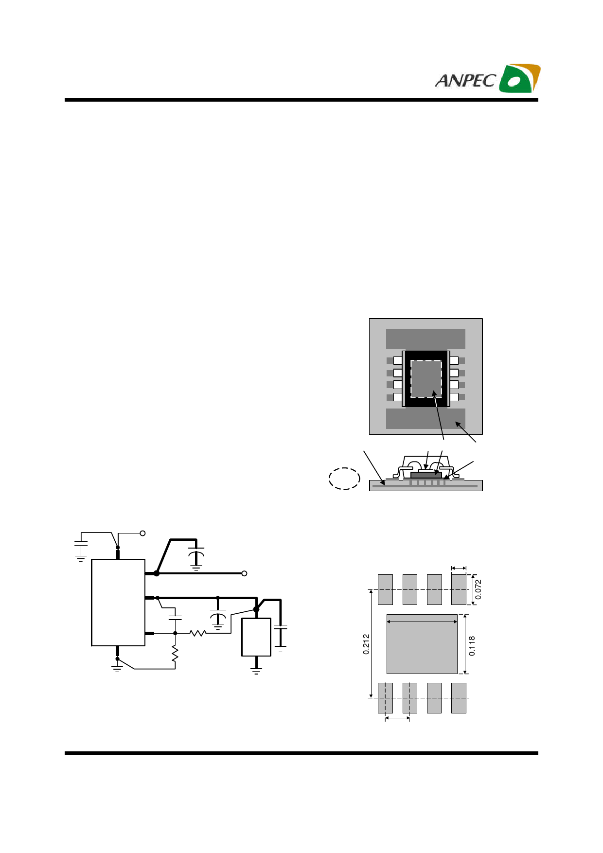
Thermal Consideration
Refer to the figure 2, the SOP-8P is a cost-effective pack-
age featuring a small size like a standard SOP-8 and a
bottom exposed pad to minimize the thermal resistance
of the package, being applicable to high current
applications. The exposed pad must be soldered to the
top-layer ground plane. It is recommended to connect the
top-layer ground pad to the internal ground plan by using
vias. The copper of the ground plane on the top-layer con-
ducts heat into the PCB and ambient air. Please enlarge
the area of the top-layer pad and the ground plane to
reduce the case-to-ambient resistance (θCA).
1
8
2
7
SOP-8P
3
6
4
5
Internal
ground
plane
Ambient
Air
Exposed
Die Pad
Top
ground
plane
PCB
Figure 2
Recommanded Minimum Footprint
0.024
8765
0.138
Figure 1
12
0.050
34
Unit : Inch
Copyright © ANPEC Electronics Corp.
12
Rev. A.3 - Jun., 2009
www.anpec.com.tw
Share Link: 