AD6672 Ver la hoja de datos (PDF) - Analog Devices
Número de pieza
componentes Descripción
Fabricante
AD6672 Datasheet PDF : 30 Pages
| |||
Data Sheet
AD6672
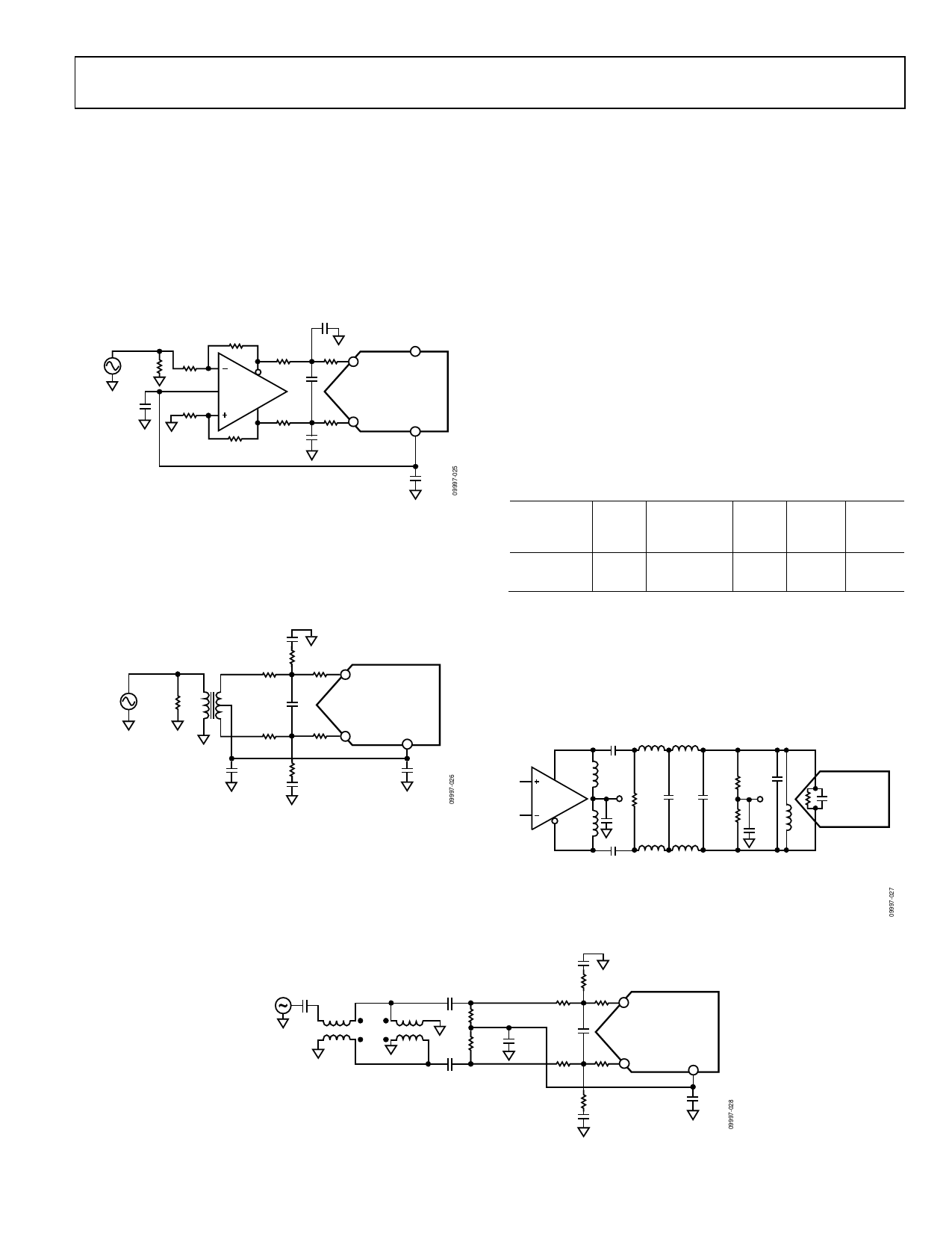
Differential Input Configurations
Optimum performance can be achieved when driving the AD6672
in a differential input configuration. For baseband applications, the
AD8138, ADA4937-1, and ADA4930-1 differential drivers provide
excellent performance and a flexible interface to the ADC.
The output common-mode voltage of the ADA4930-1 is easily
set with the VCM pin of the AD6672 (see Figure 25), and the
driver can be configured in a Sallen-Key filter topology to
provide band-limiting of the input signal.
15pF
VIN
76.8Ω
0.1µF
200Ω
90Ω
33Ω
15Ω
5pF
ADA4930-1
120Ω
200Ω
33Ω
15Ω
15pF
VIN– AVDD
ADC
VIN+
VCM
0.1µF
Figure 25. Differential Input Configuration Using the ADA4930-1
For baseband applications where SNR is a key parameter,
differential transformer coupling is the recommended input
configuration. An example is shown in Figure 26. To bias the
analog input, connect the VCM voltage to the center tap of the
secondary winding of the transformer.
2V p-p
49.9Ω
C2
R3
R2
VIN+
R1
C1
ADC
R1
R2
VIN–
VCM
the true SNR performance of the AD6672. For applications where
SNR is a key parameter, differential double balun coupling is
the recommended input configuration (see Figure 28). In this
configuration, the input is ac-coupled and the VCM voltage is
provided to the input through a 33 Ω resistor. This resistor
compensates for losses in the input baluns to provide a 50 Ω
impedance to the driver.
In the double balun and transformer configurations, the value
of the input capacitors and resistors is dependent on the input
frequency and source impedance. Based on these parameters,
the value of the input resistors and capacitors may need to be
adjusted or some components may need to be removed. Table 9
displays recommended values to set the RC network for
different input frequency ranges. However, these values are
dependent on the input signal and bandwidth and should be
used only as a starting guide. Note that the values given in Table 9
are for each R1, R2, C2, and R3 component shown in Figure 26
and Figure 28.
Table 9. Example RC Network
Frequency
Range
(MHz)
R1
C1
Series Differential
(Ω) (pF)
0 to 100 33
8.2
100 to 300 15
3.9
R2
Series
(Ω)
0
0
C2
Shunt
(pF)
15
8.2
R3
Shunt
(Ω)
49.9
49.9
An alternative to using a transformer-coupled input at
frequencies in the second Nyquist zone is to use an amplifier
with variable gain. The AD8375 digital variable gain amplifier
(DVGA) provides good performance for driving the AD6672.
Figure 27 shows an example of the AD8375 driving the AD6672
through a band-pass antialiasing filter.
1000pF 180nH 220nH
0.1µF
R3
C2
0.1µF
Figure 26. Differential Transformer-Coupled Configuration
The signal characteristics must be considered when selecting a
transformer. Most RF transformers saturate at frequencies
below a few megahertz. Excessive signal power can also cause
core saturation, which leads to distortion.
At input frequencies in the second Nyquist zone and above, the
noise performance of most amplifiers is not adequate to achieve
2V p-p
0.1µF
PA
SS
0.1µF
33Ω
P
0.1µF 33Ω
1µH
AD8375
1µH
VPOS
301Ω
1nF
165Ω
5.1pF 3.9pF
165Ω
15pF
VCM
1nF
AD6672
2.5kΩ║2pF
68nH
NOTES
1000pF 180nH 220nH
1. ALL INDUCTORS ARE COILCRAFT® 0603CS COMPONENTS
WITH THE EXCEPTION OF THE 1µH CHOKE INDUCTORS (0603LS).
2. FILTER VALUES SHOWN ARE FOR A 20MHz BANDWIDTH FILTER
CENTERED AT 140MHz.
Figure 27. Differential Input Configuration Using the AD8375
C2
R3
R1
R2
VIN+
C1
0.1µF
R1
R2
ADC
VIN–
VCM
R3
C2
Figure 28. Differential Double Balun Input Configuration
Rev. C | Page 17 of 30
0.1µF
Share Link: 