AD6672(Rev0) Ver la hoja de datos (PDF) - Analog Devices
Número de pieza
componentes Descripción
Fabricante
AD6672 Datasheet PDF : 32 Pages
| |||
AD6672
THEORY OF OPERATION
The AD6672 can sample any fS/2 frequency segment from dc to
250 MHz using appropriate low-pass or band-pass filtering at
the ADC inputs with little loss in ADC performance.
Programming and control of the AD6672 are accomplished
using a 3-pin, SPI-compatible serial interface.
ADC ARCHITECTURE
The AD6672 architecture consists of a front-end sample-and-
hold circuit, followed by a pipelined switched-capacitor ADC.
The quantized outputs from each stage are combined into a
final 11-bit result in the digital correction logic. The pipelined
architecture permits the first stage to operate on a new input
sample and the remaining stages to operate on the preceding
samples. Sampling occurs on the rising edge of the clock.
Each stage of the pipeline, excluding the last, consists of a low
resolution flash ADC connected to a switched-capacitor digital-
to-analog converter (DAC) and an interstage residue amplifier
(MDAC). The MDAC magnifies the difference between the
reconstructed DAC output and the flash input for the next stage
in the pipeline. One bit of redundancy is used in each stage to
facilitate digital correction of flash errors. The last stage simply
consists of a flash ADC.
The input stage of the AD6672 contains a differential sampling
circuit that can be ac- or dc-coupled in differential or single-
ended modes. The output staging block aligns the data, corrects
errors, and passes the data to the output buffers. The output
buffers are powered from a separate supply, allowing digital
output noise to be separated from the analog core. During
power-down, the output buffers go into a high impedance state.
The AD6672 features a noise shaping requantizer (NSR) to
allow higher than 11-bit SNR to be maintained in a subset of
the Nyquist band.
ANALOG INPUT CONSIDERATIONS
The analog input to the AD6672 is a differential switched-
capacitor circuit that has been designed to attain optimum
performance when processing a differential input signal.
The clock signal alternatively switches the input between
sample mode and hold mode (see the configuration shown in
Figure 24). When the input is switched into sample mode, the
signal source must be capable of charging the sampling
capacitors and settling within 1/2 clock cycle.
A small resistor in series with each input can help reduce the
peak transient current required from the output stage of the
driving source. A shunt capacitor can be placed across the
inputs to provide dynamic charging currents. This passive
network creates a low-pass filter at the ADC input; therefore,
the precise values are dependent on the application.
In intermediate frequency (IF) undersampling applications, the
shunt capacitors should be reduced. In combination with the
driving source impedance, the shunt capacitors limit the input
bandwidth. Refer to the AN-742 Application Note, Frequency
Domain Response of Switched-Capacitor ADCs; the AN-827
Application Note, A Resonant Approach to Interfacing Amplifiers
to Switched-Capacitor ADCs; and the Analog Dialogue article,
“Transformer-Coupled Front-End for Wideband A/D Converters,”
for more information on this subject.
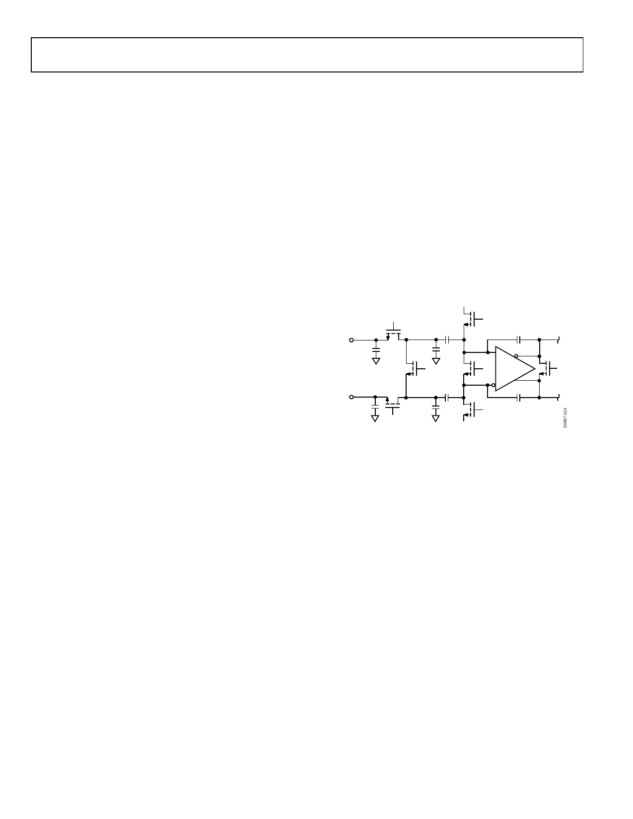
BIAS
VIN+
CPAR1
S
CS
CPAR2
S
CFB
H
S
S
VIN–
CPAR1
CS
CPAR2
S
CFB
S
BIAS
Figure 24. Switched-Capacitor Input
For best dynamic performance, match the source impedances
driving VIN+ and VIN− and differentially balance the inputs.
Input Common Mode
The analog inputs of the AD6672 are not internally dc biased.
In ac-coupled applications, the user must provide this bias
externally. Setting the device so that VCM = 0.5 × AVDD (or
0.9 V) is recommended for optimum performance. An on-
board common-mode voltage reference is included in the
design and is available from the VCM pin. Using the VCM
output to set the input common mode is recommended.
Optimum performance is achieved when the common-mode
voltage of the analog input is set by the VCM pin voltage
(typically 0.5 × AVDD). The VCM pin must be decoupled to
ground by a 0.1 μF capacitor, as described in the Applications
Information section. Place this decoupling capacitor close to the
pin to minimize the series resistance and inductance between
the part and this capacitor.
Rev. 0 | Page 16 of 32
Share Link: 