3544L_OLD Ver la hoja de datos (PDF) - Unisonic Technologies
Número de pieza
componentes Descripción
Fabricante
3544L_OLD Datasheet PDF : 9 Pages
| |||
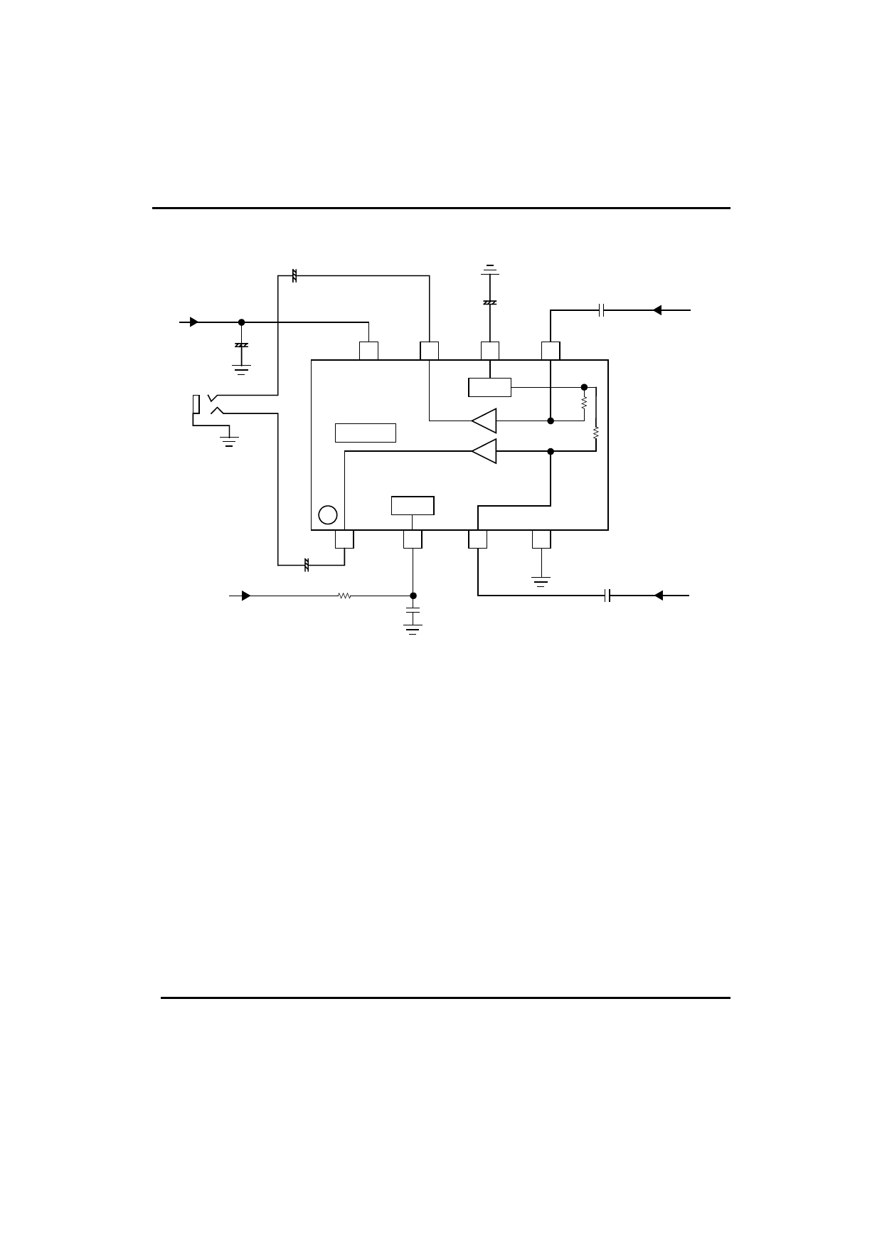
UTC 3544 LINEAR INTEGRATED CIRCUIT
APPLICATION EXAMPLE
330μ
Vcc
+
+
1μ
+ 47μ
Vcc
8
OUT2
7
BIA
S
6
IN2
5
VIN2
TSD
BIAS
6dB
+
+
6dB
90K
90K
VMUTE
H:Active
L:Mute
MUTE
1
OUT1
+
2
MUTE
3
IN1
100k
1μ
4
GND
1μ
VIN1
EXPLANATION OF EXTERNAL XOMPONENTS
(1)Input coupling capacitor(C3 and C5)
Determined by the low-band cut-off frequency.Since the input impedance for this IC is 180kΩ,it can be
determined by the formula below,but take into consideration the fluctuations,ambent temperature,etc.(a
multi-layered ceramic capacitor is recommended).
C3(C5)=1/(2π×180kΩ×f)
(2)BIAS capacitor(C6)
47μF when Vcc=5V,and 33μF when Vcc=3V.If the capacitance is lowered too much,the electrical
characteristics will be adversely affected and popping noise may occur.Therefore,take th sufficient considerations
before changing these values.
(3)MUTE pin for anti-pop measures(R2 and C2)
Possesses an impedance of 190kΩ with respect to GND,so if R2 is increased too much,the MUTE mode may
become unable to be released.
(4)Output coupling capacitor(C1 and C7)
Determined by the low-band cutoff frequency.As the output load resistance value RL(assuming that for output
protection or current limiting,a resistor Rx will be inserted),it can be determined by the formula below.
C1(C7)=1/(2π×(RL+Rx) ×f)
(5)Input gain adjustment resistor(R3 and R4)
Input gain adjustment can by performed by extemal resistors R3 and R4,The desired gain can be set by the
formula givev below.
Gvc=6+20log(90kΩ/(90kΩ+R3))[ dB ]
UTC UNISONIC TECHNOLOGIES CO. LTD 6
QW-R107-040,A
Share Link: 