INA-51063-TR1 Ver la hoja de datos (PDF) - HP => Agilent Technologies
Número de pieza
componentes Descripción
Fabricante
INA-51063-TR1 Datasheet PDF : 5 Pages
| |||
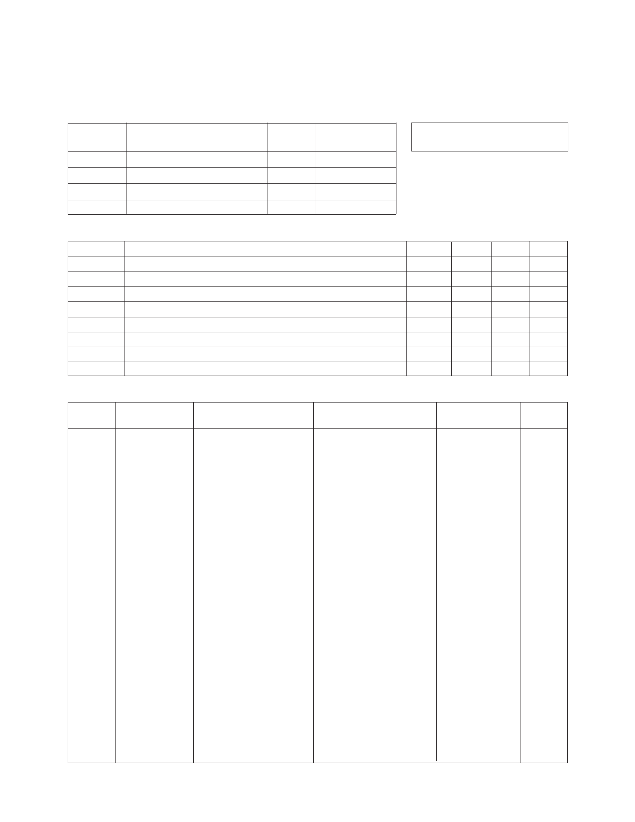
Absolute Maximum Ratings
Symbol
VCC
Pin
Tj
TSTG
Parameter
Supply Voltage, to ground
CW RF Input Power
Junction Temperature
Storage Temperature
Units
V
dBm
°C
°C
Absolute
Maximum[1]
12
+13
150
-65 to 150
Thermal Resistance[2]:
θjc = 200°C/W
Notes:
1. Operation of this device above any one
of these limits may cause permanent
damage.
2. TC = 25°C (TC is defined to be the
temperature at the package pins where
contact is made to the circuit board)
INA-51063 Electrical Specifications[3], TC = 25°C, ZO = 50 Ω ,VCC = 5 V
Symbol
Parameters and Test Conditions
Units Min.
Typ. Max.
Gp
Power Gain (|S21|2)
NF
Noise Figure
f = 1500 MHz
dB 18
20.5
f = 1500 MHz
dB
3
P1dB
Output Power at 1 dB Gain Compression f = 1500 MHz dBm
-2.5
IP3
Third Order Intercept Point
f = 1500 MHz dBm
+6
VSWR Input VSWR
f = 1500 MHz
1.3
Output VSWR
f = 1500 MHz
1.8
Icc
Device Current
ιd
Group Delay
mA
f = 1500 MHz
ps
12 14
240
INA-51063 Typical Scattering Parameters[3], TC = 25°C, ZO = 50 Ω ,VCC = 5.0 V
Freq.
GHz
S11
Mag Ang dB
S21
Mag
Ang dB
S12
Mag Ang
S22
Mag Ang
0.05
0.17 177 20.8 10.94 -4 -30.9 0.029 -1
0.23
-5
0.10
0.17 175 20.8 10.95 -7 -30.8 0.029 -2
0.23
-8
0.20
0.16 170 20.8 10.94 -14 -30.9 0.028 -4
0.23 -16
0.30
0.16 166 20.7 10.89 -21 -31.0 0.028 -5
0.23 -25
0.40
0.14 162 20.8 10.94 -28 -31.2 0.028 -7
0.24 -33
0.50
0.13 159 20.8 10.96 -35 -31.3 0.027 -9
0.24 -43
0.60
0.12 158 20.8 11.00 -42 -31.5 0.027 -10
0.24 -52
0.70
0.10 158 20.9 11.06 -49 -31.6 0.026 -12
0.24 -61
0.80
0.08 164 20.9 11.06 -57 -31.9 0.026 -14
0.25 -69
0.90
0.07 172 20.9 11.10 -64 -32.1 0.025 -15
0.26 -77
1.00
0.07 -174 20.9 11.10 -72 -32.5 0.024 -17
0.26 -85
1.10
0.07 -156 20.9 11.14 -80 -32.7 0.023 -18
0.27 -94
1.20
0.08 -142 20.9 11.11 -88 -33.2 0.022 -21
0.27 -103
1.30
0.10 -135 20.9 11.08 -96 -33.5 0.021 -23
0.28 -113
1.40
0.12 -131 20.8 11.01 -105 -33.9 0.020 -25
0.28 -122
1.50
0.14 -131 20.7 10.88 -113 -34.6 0.019 -28
0.28 -131
1.60
0.17 -132 20.6 10.71 -122 -35.2 0.017 -30
0.28 -140
1.70
0.19 -134 20.4 10.45 -131 -36.0 0.016 -33
0.28 -150
1.80
0.22 -135 20.1 10.16 -139 -36.8 0.014 -36
0.27 -159
1.90
0.24 -139 19.8 9.78 -148 -37.8 0.013 -39
0.27 -168
2.00
0.26 -142 19.4 9.37 -157 -39.1 0.011 -42
0.25 -177
2.10
0.28 -145 19.0 8.90 -165 -40.6 0.009 -47
0.24 175
2.20
0.30 -148 18.5 8.42 -174 -42.2 0.008 -53
0.22 166
2.30
0.32 -151 18.0 7.96 179 -44.3 0.006 -63
0.21 158
2.40
0.33 -154 17.4 7.45 171 -46.7 0.005 -79
0.20 150
2.50
0.35 -157 16.9 6.98 164 -48.9 0.004 -108 0.18 143
3.00
0.41 -169 13.8 4.89 133 -39.0 0.011 163 0.10 115
3.50
0.45 -179 10.8 3.48 108 -31.9 0.025 146 0.03 123
4.00
0.50 172 8.3
2.59 88 -26.9 0.045 132 0.05 -132
Note:
3. Reference plane per Figure 9 in Applications Information section.
6-152
K
Factor
1.65
1.65
1.70
1.70
1.69
1.74
1.74
1.79
1.78
1.83
1.89
1.95
2.02
2.10
2.19
2.31
2.57
2.77
3.20
3.53
4.32
5.49
6.49
9.03
11.51
15.20
7.64
4.61
3.29
Share Link: 