S-80717AL-AE-X Ver la hoja de datos (PDF) - Seiko Instruments Inc
Número de pieza
componentes Descripción
Fabricante
S-80717AL-AE-X Datasheet PDF : 42 Pages
| |||
HIGH-PRECISION VOLTAGE DETECTOR
S-807 Series
Operation
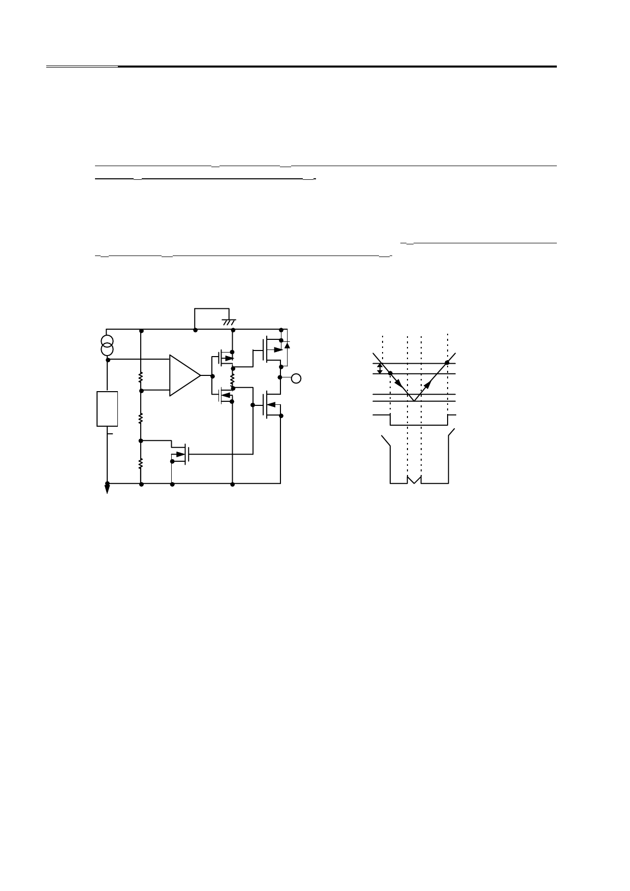
1. Basic operation
(1) When power supply voltage VDD is greater than the release voltage +VDET, the Nch transistor is OFF and the Pch
transistor ON, causing VDD (high) to appear at the output. With the Nch transistor of Figure 13 (a) off, the comparator
input voltage is (RB+RC)/(RA+RB+RC)×VDD.
(2) When power supply voltage VDD goes below +VDET, the output continues to maintain the power supply voltage level, as
long as VDD remains above the detection voltage -VDET. When VDD does fall below -VDET (A in Figure 14), the Nch
transistor goes ON, the Pch transistor goes OFF, and VSS appears at the output. With the Nch transistor of Figure 13
(a) ON, the comparator input voltage is RB/(RA+RB)×VDD.
(3) When VDD falls below the minimum operating voltage, the output becomes undefined. However, output will revert to VDD
if a pull-up has been employed.
(4) VSS will again be output when VDD rises above the minimum operating voltage. VSS will continue to be output even when
VDD surpasses -VDET, as long as it does not exceed the release voltage +VDET.
(5) When VDD rises above +VDET (B in Figure 14), the Nch transistor goes OFF, the Pch transistor goes ON, and VDD
appears at the output.
VDD
-
RA
+
RB
VREF
(a)
RC
*
Pch
OUT
Nch
VSS
* Parasitic diode
Figure 13
(1) (2) (3) (4) (5)
VDD
Hysteresis
A
width
(VHYS)
B Release voltage(+VDET)
Detection voltage(-VDET)
Minimum operating
voltage
VSS
Comparator
output
VDD
OUT
VSS
Figure 14
26
Seiko Instruments Inc.
Share Link: 