HMA510JC-55 Ver la hoja de datos (PDF) - Intersil
Número de pieza
componentes Descripción
Fabricante
HMA510JC-55 Datasheet PDF : 10 Pages
| |||
HMA510
Functional Description
The HMA510 is a high speed 16 x 16-bit multiplier accumu-
lator (MAC). It consists of a 16-bit parallel multiplier follower
by a 35-bit accumulator. All inputs and outputs are regis-
tered and are latched on the rising edge of the associated
clock signal. The HMA510 is divided into four sections: the
input section, the multiplier array, the accumulator and the
output/preload section.
The input section has two 16-bit Operand Input Registers for
the X and Y operands which are latched on the rising edge
of CLKX and CLKY respectively. A four bit Control Register
(TC, RND, ACC, SUB) is also included and is latched from
either of the input clock signals.
The 16 x 16 multiplier array produces the 32-bit product of
the input operands. Two's complement or unsigned magni-
tude operation can be selected by the use of the TC control.
The 32-bit result may also be rounded through the use of the
RND control. In this case, a ‘1’ is added to the MSB of the
LSP (bit P15). The 32-bit product is zero-filled or sign-
extended as appropriate and passed as a 35-bit number to
the accumulator section.
The accumulator functions are controlled by the ACC, SUB
and PREL control inputs. Four functions may be selected:
the accumulator may be loaded with the current product; the
product may be added to the accumulator contents; the
accumulator contents may be subtracted from the current
product; or the accumulator may be loaded from the bidirec-
tional ports. The Accumulator Registers are updated at the
rising edge of the CLKP signal.
The output/preload section contains the Accumulator/Output
Register and the bidirectional ports. This section is con-
trolled by the signals PREL, OEX, OEM and OEL. When
PREL is high, the output buffers are in a high impedance
state. When one of the controls OEX, OEM or OEL are also
high, data present at the outputs will be preloaded into the
associated register on the rising edge of CLKP. When PREL
is low, the signals OEX, OEM and OEL are enable controls
for their respective three-state output ports.
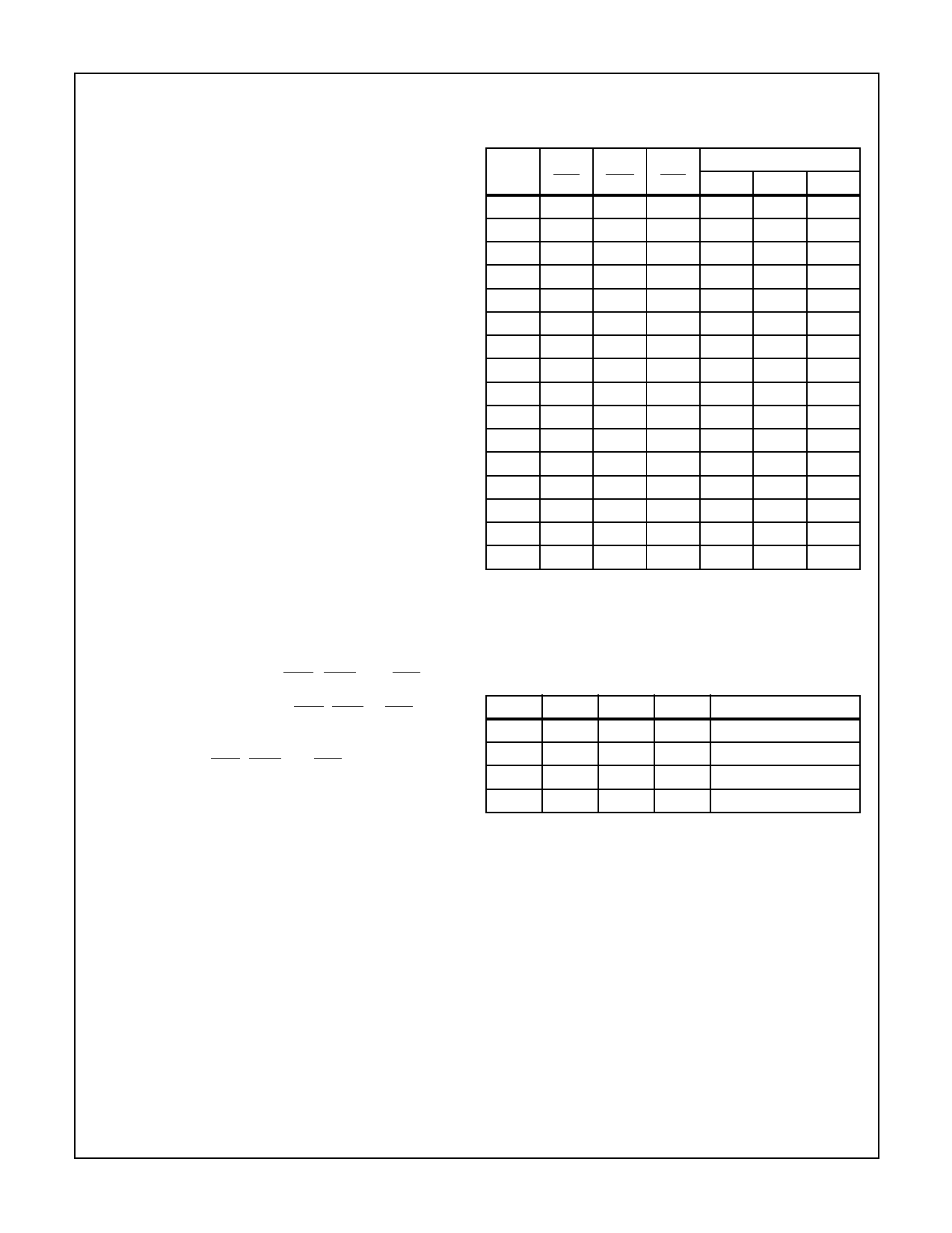
TABLE 1. PRELOAD FUNCTION TABLE
OUTPUT REGISTERS
PREL OEX OEM OEL XTP MSP LSP
0
0
0
0
Q
Q
Q
0
0
0
1
Q
Q
Z
0
0
1
0
Q
Z
Q
0
0
1
1
Q
Z
Z
0
1
0
0
Z
Q
Q
0
1
0
1
Z
Q
Z
0
1
1
0
Z
Z
Q
0
1
1
1
Z
Z
Z
1
0
0
0
Z
Z
Z
1
0
0
1
Z
Z
PL
1
0
1
0
Z
PL
Z
1
0
1
1
Z
PL
PL
1
1
0
0
PL
Z
Z
1
1
0
1
PL
Z
PL
1
1
1
0
PL
PL
Z
1
1
1
1
PL
PL
PL
Z = Output Buffers at High Impedance (Disabled).
Q = Output Buffers at LOW Impedance. Contents of Output Reg-
ister Available Through Output Ports.
PL = Output disabled. Preload data supplied to the output pins will
be loaded into the register at the rising edge of CLKP.
TABLE 2. ACCUMULATOR FUNCTION TABLE
PREL
L
L
L
H
ACC
L
H
H
X
SUB
X
L
H
X
P
OPERATION
Q Load
Q Add
Q Subtract
PL Preload
4
Share Link: 